


Semiconductor component manufacturing involves a series of complex production processes to transform raw materials into finished components for various applications that provide critical control and sensing functions.
Semiconductor manufacturing involves a series of complex processes to transform raw materials into final finished components. The semiconductor manufacturing process generally includes four main stages: wafer manufacturing, wafer test assembly or packaging, and final testing. Each stage has its own unique challenges and opportunities.
The semiconductor manufacturing process also faces many challenges including cost, complexity, diversity and yield, but also brings great opportunities for innovation and development. By addressing the difficulties and seizing the opportunities, we can promote the development of new technologies to change the way we live and work, while enabling the industry to continue to develop and grow.

一. Overview of semiconductor manufacturing process
The process of manufacturing semiconductors can be divided into the following key steps.
1. Wafer preparation
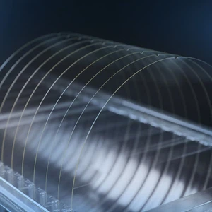
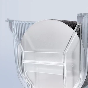
Silicon wafers are selected as the starting material for the semiconductor process. The wafers are cleaned, polished, and prepared for use as substrates for manufacturing electronic components.
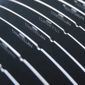
2. Patterning
In this process, patterns are created on silicon wafers using a process called photolithography. A layer of corrosion-resistant photoresist is applied to the surface of the wafer, and then a mask is placed on top of the wafer. The mask has a pattern corresponding to the relevant pre-manufactured electronic components. The pattern is then transferred from the mask to the photoresist layer using ultraviolet light. The exposed photoresist areas are then removed, leaving a patterned surface on the wafer.
3. Material doping
In this step, materials are added to the silicon wafer to change its electrical properties. The most commonly used materials are boron or phosphorus, which can be added in small amounts to produce p-type or n-type semiconductors, respectively. These materials are implanted into the surface of the wafer using ion acceleration in a process called ion implantation.
4. Wafer deposition processing
During this process, thin film materials are deposited on a wafer to create electronic components. This can be achieved through a variety of techniques, including chemical vapor deposition (CVD), physical vapor deposition (PVD), and atomic layer deposition (ALD). These processes can be used to deposit materials such as metals, oxides, and nitrides.
5. Etching
Removing part of the material from the surface of the wafer to produce the shape and structure required for the electronic component. Etching can be performed using a variety of techniques, including wet etching, dry etching, and plasma etching. These processes use chemicals or plasma to selectively remove specific materials from the wafer.
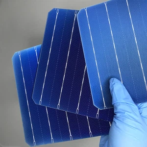
6. Packaging
Electronic components are packaged into a final product that can be used in electronic devices. This includes connecting the components to a substrate such as a printed circuit board, and then connecting them to other components using wires or other means. Semiconductor processes are very complex and involve a variety of specialized equipment and materials. These processes are essential to the manufacture of modern electronic devices and continue to evolve with the iteration of new technologies.
Typically, the process of producing semiconductor chips takes a few weeks to a few months. Starting from the first stage, a silicon wafer needs to be manufactured to serve as the substrate for the chip. This process typically includes the following processes, cleaning, deposition, lithography, etching and doping. The wafer may need to undergo hundreds of different process operations, so the entire wafer manufacturing process may take up to 16-18 weeks.
Once the individual chips are manufactured on the wafer, they need to be separated and packaged into individual units. This also includes testing each chip to ensure that it meets the specifications, and then separating it from the wafer and mounting it on the package or substrate. After the chips are packaged, they will go through a rigorous testing process to ensure that they meet quality standards and achieve the expected functions. This includes running electronic tests, functional tests, and other types of verification tests to identify any defects or problems. This also depends on the complexity of the chip and the required testing requirements, so this packaging and testing process can take 8-10 weeks.
All in all, the entire process of producing semiconductor chips can take several weeks or months, because it depends on the relevant technologies used and the complexity of the chip design.

二. Trends and Challenges in Semiconductor Manufacturing
1. Pattern Transfer
Advances in pattern transfer technology have become a key driver of the rapid development of the semiconductor industry, enabling the manufacture of smaller and more complex electronic components.
A major advance in pattern transfer technology is the development of advanced lithography, which is the process of transferring patterns to a medium using light or other radiation sources. In particular, lithography technologies developed in recent years, such as extreme ultraviolet (EUV) lithography and multiple patterning technology, are used to produce smaller and more complex graphics.
EUV lithography uses extremely short-wavelength beams of light to create extremely precise patterns on silicon wafers. This technology can create sizes as small as a few nanometers, which is essential for the manufacture of advanced electronic components such as microprocessors.
Multiple patterning is another lithography technology that can create smaller patterns. This technology involves breaking down a single pattern into multiple micro-polar patterns and then transferring them to the surface of the wafer. As a result, the created pattern can be smaller than the wavelength of radiation used in lithography.
2. Doping
Dopants are the addition of specific media to silicon wafers to change their electrical properties. Advances in doping technology have been a key factor in the rapid development of the semiconductor industry. This technological advancement is due to the emergence of new dielectric materials.
Traditionally, boron and phosphorus are the most commonly used doping materials because they can produce p-type and n-type semiconductors, respectively. However, in recent years, new materials such as germanium, arsenic and antimony have been developed and can be used to manufacture more complex electronic components.
Another advancement in doping technology is the advancement of more precise doping processes. In the past, ion implantation was the main technology used for doping, involving the use of high-speed ions to implant dielectrics into the surface of the wafer. Although ion implantation is still commonly used, new technologies such as molecular beam epitaxy (MBE) and chemical vapor deposition (CVD) have been developed to enable more precise control of the doping process.
3. Deposition
Deposition is another key process in semiconductor manufacturing, which involves depositing a thin film of material onto a substrate. This process can be achieved through various technologies, such as physical vapor deposition (PVD), chemical vapor deposition (CVD), atomic layer deposition (ALD), etc.
At the same time, new technologies are also constantly developing, including metal organic chemical vapor deposition (MOCVD), plasma enhanced deposition, roll-to-roll deposition, etc.
4. Etching
Etching involves removing specific parts of semiconductor materials to create patterns or structures. Advances in etching technology are the main reason for the rapid development of the semiconductor industry and are also a key technology for manufacturing smaller and more complex electronic components.
In the past, wet etching was the main technology commonly used, which involves immersing the wafer in a solution that dissolves the material. However, wet etching is not precise and can cause damage to adjacent structures.
The emergence of dry etching technology has enabled more precise and highly controllable etching production, such as reactive ion etching (RIE) and plasma etching. RIE is a technology that uses reactive ions to selectively remove material from a wafer, allowing precise control of the etching process.
Plasma etching is a similar technology that uses gas plasma to remove material, but it has the additional benefit of selectively removing specific materials, such as metals or silicon.

5. Packaging
The packaging process in semiconductor manufacturing involves encapsulating an integrated circuit in a protective casing that also provides electrical connections to the outside world. The packaging process affects the performance, reliability, and cost of the final product.
3D packaging involves stacking multiple chips together to create high-density integrated circuits. This technology can reduce the overall size of the device and improve its performance while also reducing power consumption.
Fan-out packaging is a technology that embeds integrated circuits in a layer of epoxy molding compound, using copper pillars fanned out from the chip for electrical connections. This technology enables high-density packaging in a smaller size.
System-in-Package (SiP) is another technology that integrates multiple chips, sensors, and other components into a single package. It can reduce the overall size of the device while also improving its overall performance.


