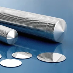
The substrate is the physical basis of the device and determines the feasibility and cost of epitaxial growth.
The epitaxial layer is the functional core, and the electrical and optical performance are optimized through structural design and precise doping.
The matching of the two (lattice, heat, electricity) is the key to high-performance devices, driving semiconductor technology to higher frequency, higher power, and lower power consumption.
1. Substrate
Definition and function
Physical support: The substrate is the carrier of the semiconductor device, usually a round or square single crystal thin sheet (such as silicon wafer).
Crystal template: Provides a template for atomic arrangement for epitaxial layer growth to ensure that the epitaxial layer is consistent with the substrate crystal structure (homogeneous epitaxy) or matches (heterogeneous epitaxy).
Electrical basis: Some substrates directly participate in device conduction (such as silicon-based power devices) or serve as insulators to isolate circuits (such as sapphire substrates).
2. Comparison of mainstream substrate materials
| Material | Properties | Typical Applications |
| silicon(Si) | Low cost, mature technology, medium thermal conductivity | integrated circuit,MOSFET,IGBT |
| sapphire(Al₂O₃) | insulation,High temperature resistance, large lattice mismatch (up to 13% with GaN) | GaN-based LEDs and RF devices |
| Silicon Carbide(SiC) | High thermal conductivity, high breakdown field strength, high temperature resistance | Electric vehicle power modules, 5G base station RF devices |
| Gallium Arsenide (GaAs) | Excellent high frequency characteristics, direct bandgap | RF chips, laser diodes, solar cells |
| Gallium Nitride (GaN) | High electron mobility, high voltage resistance | Fast charging adapter, millimeter wave communication device |
3. Core considerations for substrate selection
Lattice matching: Reduce epitaxial layer defects (such as GaN/sapphire lattice mismatch of 13%, requiring a buffer layer).
Matching thermal expansion coefficient: avoid stress cracking caused by temperature changes.
Cost and process compatibility: For example, silicon substrates dominate the mainstream due to mature processes.

2. Epitaxial Layer
1. Definition and purpose
Epitaxial growth: Deposit single crystal thin films on the substrate surface by chemical or physical methods, and the atomic arrangement is strictly aligned with the substrate.
Core role:
Improve material purity (the substrate may contain impurities).
Construct heterogeneous structures (such as GaAs/AlGaAs quantum wells).
Isolate substrate defects (such as micropipe defects in SiC substrates).
2. Classification of epitaxial technology

3. Key parameters of epitaxial layer design
Thickness: from a few nanometers (quantum wells) to tens of microns (power device epitaxial layer).
Doping: Precisely control the carrier concentration by doping impurities such as phosphorus (N-type) and boron (P-type).
Interface quality: Lattice mismatch needs to be alleviated by buffer layers (such as GaN/AlN) or strained superlattices.
4. Challenges and solutions of heteroepitaxial growth Lattice mismatch:
Gradual buffer layer: Gradually change the composition from substrate to epitaxial layer (such as AlGaN gradient layer).
Low-temperature nucleation layer: Grow thin layers at low temperature to reduce stress (such as low-temperature AlN nucleation layer of GaN).
Thermal mismatch: Select a combination of materials with similar thermal expansion coefficients, or use a flexible interface design.

3. Collaborative application cases of substrate and epitaxy
Case 1: GaN-based LED substrate: sapphire (low cost, insulation).
Epitaxial structure:
Buffer layer (AlN or low-temperature GaN) → Reduce lattice mismatch defects.
N-type GaN layer → Provide electrons.
InGaN/GaN multiple quantum wells → Light-emitting layer.
P-type GaN layer → Provide holes.
Result: Defect density is as low as 10⁸ cm⁻², and luminous efficiency is significantly improved.

Case 2: SiC power MOSFET
Substrate: 4H-SiC single crystal (withstand voltage up to 10 kV).
Epitaxial layer:
N-type SiC drift layer (thickness 10-100 μm) → withstand high voltage.
P-type SiC base region → control channel formation.
Advantages: 90% lower on-resistance than silicon devices, 5 times faster switching speed.
Case 3: Silicon-based GaN RF device substrate: high-resistance silicon (low cost, easy integration).

Epilayer: AlN nucleation layer → alleviate the lattice mismatch between Si and GaN (16%).
GaN buffer layer → capture defects and prevent them from extending to the active layer.
AlGaN/GaN heterojunction → form a high electron mobility channel (HEMT).
Application: 5G base station power amplifier, frequency can reach more than 28 GHz.


