






Ningbo Sibranch Microelectronics Technology Co.,Ltd.:Your Trustworthy 300mm Silicon Wafer Manufacturer!
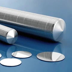
Founded in 2006 by material science and engineering scientist in Ningbo, China, Sibranch Microelectronics aims to provide semiconductor wafer and service all over the world. Our main products include standard silicon wafers SSP (single side polished), DSP (Double side polished), test silicon wafers and prime silicon wafers, SOI (Silicon on Insulator) wafer and coin roll wafers with diameter up to 12 inch, CZ/MCZ/FZ/NTD, almost any orientation, off cut, high and low resistivity, ultra-flat, ultra-thin, thick wafers etc.
Leading Service
We are committed to constantly innovating our products to provide foreign customers with a large number of high-quality products to exceed customer satisfaction. We can also provide customized services according to customers' requirements such as size, color, appearance, etc. We can provide the most favorable price and high-quality products.
Quality Guaranteed
We have been continuously researching and innovating to meet the needs of different customers. At the same time, we always adhere to strict quality control to ensure that the quality of every product meets international standards.
Wide Sales Countries
We focus on sales in overseas markets. Our products are exported to Europe, America, Southeast Asia, the Middle East and other regions, and are well received by customers around the world.
Various Types of Products
Our company offers customized silicon wafer processing services tailored to meet the specific needs of our clients. These include Si Wafer BackGrinding, Dicing, DownSizing, Edge Grinding, as well as MEMS among others. We strive to deliver bespoke solutions that exceed expectations and ensure customer satisfaction.
Product Types

CZ Silicon Wafers are cut from single crystal silicon ingots pulled using the Czochralski CZ growth method, which is most widely used in the electronics industry to grow silicon crystals from large cylindrical silicon ingots used to manufacture semiconductor devices. In this process, an elongated crystalline silicon seed with precise orientation tolerance is introduced into a silicon molten pool with precisely controlled temperature. The seed crystal is slowly pulled upward from the melt at a strictly controlled rate, and crystal solidification of the liquid phase atoms occurs at the interface. During this pulling process, the seed crystal and the crucible rotate in opposite directions, forming a large single crystal silicon with a perfect crystal structure of the seed.

Silicon oxide wafer is an advanced and essential material used in various high-tech industries and applications. It is a high-purity crystalline substance produced by processing high-quality silicon materials, making it an ideal substrate for many different types of electronic and photonic applications.

Dummy wafers (also called test wafers) are wafers mainly used for experiment and test and are different from general wafers for product. Accordingly, reclaimed wafers are mostly applied as dummy wafers (test wafers).

Gold-coated silicon wafers, and gold-coated silicon chips are used extensively as substrates for analytical characterization of materials. For example, materials deposited onto gold-coated wafers can be analyzed via ellipsometry, Raman spectroscopy or infrared (IR) spectroscopy due to the high-reflectivity and favorable optical properties of gold.

Silicon Epitaxial Wafers are highly versatile and can be manufactured in a range of sizes and thicknesses to suit different industry requirements. They are also used in a variety of applications, including integrated circuits, microprocessors, sensors, power electronics, and photovoltaics.

Manufactured using the latest technology and is designed to offer unparalleled reliability and consistency in performance. Thermal Oxide Dry and Wet is an essential tool for semiconductor manufacturers worldwide as it provides an efficient way to produce high-quality wafers that meet all the demanding requirements of the industry.

This wafer has a diameter of 300 millimeters, making it larger than traditional wafer sizes. This larger size makes it more cost-effective and efficient, allowing for greater production output without sacrificing quality.

The 100mm silicon wafer is a high-quality product that is widely used in the electronics and semiconductor industries. This wafer is designed to provide optimal performance, precision, and reliability that are essential in the manufacturing of semiconductor devices.

The 200mm silicon wafer is also versatile in its applications, with applications in research and development, as well as in high-volume manufacturing. It can be customized to your exact specifications, with options for thin or thick wafers, polished or unpolished surfaces, and other features based on your specific needs.
What is 300mm Silicon Wafer
A 300mm silicon wafer is a material essential for manufacturing semiconductors, which are found in all kinds of electronic devices that enrich our lives. This ultra-flat disk is polished to a mirror-like surface, and made as free as possible of tiny surface irregularities, making it the flattest object in the world. It is also ultra-clean, virtually free of microparticles and other impurities. These qualities are necessary so it can be used as the substrate material of today's state-of-the-art semiconductors.
Reliability
300mm silicon wafers are reliable in a variety of applications and are able to withstand high temperatures without diminishing their signal or power quality. That means you'll get better performance and utilize your 300mm silicon wafers for many years with less downtime than other devices.
Scalability
You can easily cut, peel, dice and shape 300mm silicon wafers into any size to fit your application needs. If Silicon comes in diameter sheets, you can use them as they come or divide them up into smaller pieces that suit your project specifications.
Expeditious Production
The process of fabricating 300mm silicon wafers is quick and easy for any size, shape, or application requirement. 300mm silicon wafers are easily cut, diced, and shaped into any size required to fit your needs.
High-speed 300mm silicon wafer fabrication
It is quite easy to fabricate 300mm silicon wafers at a very high speed compared to other products and manufacturing methods. The devices that use these wafers require high speed but also low cost of production because they are used for a wide range of applications requiring high precision such as instrumentation, communications, and microelectronics.
Properties of 300mm Silicon Wafers
300mm silicon wafers possess a unique combination of physical and chemical properties that make them ideal for use in the technology industry. These properties include electrical conductivity, thermal conductivity, and mechanical strength, among others. Understanding these properties is essential for the design and fabrication of electronic devices, as they directly impact the performance and reliability of the devices.
Electrical Properties
One of the most important properties of 300mm silicon wafers is their electrical conductivity. Silicon is a semiconductor, which means that its electrical conductivity lies between that of a conductor, like copper, and an insulator, like glass. The electrical properties of silicon can be precisely controlled by introducing small amounts of impurities, a process known as doping.
Doping involves the addition of either electron-donating elements, such as phosphorus or arsenic, or electron-accepting elements, such as boron or aluminum. The introduction of these impurities creates either an excess or a deficiency of electrons in the silicon lattice, resulting in either n-type or p-type silicon, respectively. The controlled introduction of these impurities allows for the creation of specific electrical properties in the 300mm silicon wafer, which is essential for the fabrication of semiconductor devices.
The ability to control the electrical properties of 300mm silicon wafers is crucial for the development of electronic devices, such as transistors, diodes, and integrated circuits. These devices rely on the precise control of electrical current flow, which is made possible by the unique electrical properties of 300mm silicon wafers. The performance, efficiency, and reliability of electronic devices are directly influenced by the quality and consistency of the 300mm silicon wafers used in their fabrication.
Thermal Properties
300mm silicon wafers also exhibit unique thermal properties that are critical to their function in electronic devices. One of the key thermal properties of silicon is its thermal conductivity, which is the measure of a material's ability to conduct heat. Silicon has a relatively high thermal conductivity, around 149 W/m·K at room temperature. This property is crucial in electronic devices, as it allows for the efficient dissipation of heat generated during operation, thereby preventing overheating and ensuring the reliability and longevity of the device.
Another important thermal property of silicon is its coefficient of thermal expansion (CTE), which measures how much the material expands or contracts with changes in temperature. Silicon has a relatively low CTE, around 2.6 µm/(m·K) at room temperature. This means that 300mm silicon wafers do not significantly expand or contract with temperature changes, which is important in the fabrication and operation of electronic devices. Large changes in dimension with temperature can lead to mechanical stresses and potential failure of the device.
The thermal properties of 300mm silicon wafers are not only important for the operation of the devices they are used to produce, but also for the fabrication process itself. Many steps in the fabrication process, such as doping and oxide growth, involve high temperatures. The high thermal conductivity and low CTE of 300mm silicon wafers allow these processes to be carried out efficiently and without inducing mechanical stresses in the wafer.
What Is 300mm Silicon Wafer Used for?
Semiconductor
Even though other conductors are employed in more particular applications, silicon is the best and the most used semiconductor due to its extreme mobility both at high temperatures and at room temperature. What makes Silicon an outstanding option in electronic devices is because its electrical currents can pass via the silicon conductors much quicker compared to other conductors.
300mm Silicon Wafers In Electronic Devices
Semiconductors such as the 300mm silicon wafer can be used in the production of both chips and microchips in electronic gadgets. Due to the uniqueness of the electrical currents via 300mm silicon wafers, these semiconductors are used in creating ICs (integrated circuits). The ICs act as commands for specific actions in various electronic devices.
The 300mm silicon wafer is the main element in integrated circuits. Simply put, integrated circuits are a composite of a variety of electronic elements that are brought together to perform a particular function. Silicon is the key platform for semiconductor gadgets. A wafer is just but a thin slice of the semiconductor material that acts as a substratum for microelectronic devices fitted in and above the wafer. Even if it can be simple to relate 300mm silicon wafers with very particular technological devices that individuals only dream of, 300mm silicon wafers are way much closer than anyone may think! 300mm silicon wafers are used in computers, smartphones, and mobile devices and even in the tire pressure sensor system. Manufacturing of the 300mm silicon wafer is an incredibly vital part of the establishment and expansion of a broad range of technological advancements.
In Solar Cells
300mm silicon wafers play a crucial role in the production of solar cells, which are the key components of solar panels used for harnessing solar energy. Solar cells, also known as photovoltaic cells, convert sunlight directly into electricity through the photovoltaic effect. This process involves the generation of a flow of electricity in a material upon exposure to light. The majority of solar cells are made from silicon due to its excellent semiconductor properties. Silicon's ability to absorb sunlight and its semiconductor nature makes it an ideal material for solar cells. When sunlight hits the 300mm silicon wafer in a solar cell, it excites the electrons, causing them to move and create an electric current.
There are two main types of silicon used in solar cells: monocrystalline and polycrystalline silicon. Monocrystalline silicon is made from a single crystal structure, which allows for the free and unimpeded flow of electrons, resulting in high efficiency. Polycrystalline silicon, on the other hand, is made from multiple crystal structures, which can impede the flow of electrons and result in lower efficiency, but it is cheaper to produce.
The production of 300mm silicon wafers for solar cells involves similar processes to those used in the semiconductor industry, including the wafer slicing, and polishing. However, the wafers used in solar cells are typically thicker and less pure than those used in the semiconductor industry. Despite these differences, the fundamental properties of 300mm silicon wafers, including their electrical and thermal properties, make them an essential component in the production of solar cells.
Other Uses of 300mm silicon wafers
The ultra-pure 300mm silicon wafers offer a pristine canvas on which to fabricate the integrated circuitry central to all electronics. The uses include:
- Microprocessors - The central chips powering computers and smartphones
- DRAM & flash memory - Billions of silicon-based memory cells on chips
- CMOS sensors - Image sensors capturing light in smartphone cameras and more
- Power devices - Specialized designs managing electricity in systems
- MEMS - Tiny mechanical and electromechanical silicon systems
- Optical circuits - Waveguides and photonic devices integrate optics
Frequently Asked Questions
Q: How many transistors are on a modern 300mm silicon wafer?
A: Leading edge wafers for processors like Intel's and AMD's newest chips now cram over 100 billion transistors into a single silicon die thanks to fabrication processes with features between 5-7 nanometers across.
Q: What's the largest 300mm silicon wafer size used today?
A: While the industry standard remains 300mm (12 inch) diameter wafers, a few specialty foundries like TSMC are beginning to shift small production runs to larger 450mm wafers to improve economies of scale. However, extreme technical challenges around defect rates and fabrication equipment availability currently limit mainstream adoption.
Q: How much does an individual 300mm silicon wafer cost?
A: Pricing varies tremendously based on wafer size, purity grades, surface finishing, fabrication processes, testing and more. But roughly, 200-300mm wafers range between $20 on the very low end up to $20,000 for highly exotic compound semiconductor configurations meant for specialized ASICs and space/defense applications.
Q: How are completed 300mm silicon wafers turned into end consumer chips and electronics?
A: After the wafer fabrication finishes imprinting billions of electric components as integrated circuits on the silicon surface, individual dies get cut apart and go through extensive testing, inspection, packaging into protective shells, and final distribution to electronics manufacturers who incorporate them into finished products!
Q: Could we build processors from something other than silicon in the future?
A: Research is intensely exploring new semiconductor materials like gallium nitride, carbon nanotubes, molybdenum sulfide and more. Each offers tantalizing advantages in charge velocity, thermal behaviors and computing potential. While silicon will surely continue dominating for decades longer, revolutionary new substrates will likely transform electronics again one day!
Q: What could improve 300mm silicon wafer fabrication techniques moving forward?
A: Tremendous opportunities remain to enhance precision, scale and throughput across the entire wafer production pipeline. From purification and crystal growth, to slicing, polishing and inspection, we're constantly chasing bigger wafers with smaller feature sizes and less defects through better lasers, chemical processes, automation and quality control. There's vast room left for engineering innovation!
Q: What are 300mm silicon wafers?
A: 300mm silicon wafers are thin slices of silicon that serve as the substrate for the fabrication of electronic devices. They are produced from ultra-pure silicon through a series of complex processes, including the Czochralski process, wafer slicing, and polishing.
Q: Why are 300mm silicon wafers used in the technology industry?
A: 300mm silicon wafers are used in the technology industry due to their unique electrical and thermal properties. These properties, combined with the high purity of silicon, make it an ideal material for integrated circuits and other semiconductor manufacturing, as well as solar cells.
Q: What are the challenges in 300mm silicon wafer manufacturing?
A: The production of 300mm silicon wafers involves several challenges, including maintaining the purity of the silicon throughout the production process and managing the high costs associated with the process. Solutions have been developed to address these challenges, including process optimization, silicon recycling, and the use of alternative materials.
Q: What is the future of 300mm silicon wafer production?
A: The future of 300mm silicon wafer production is likely to involve further advancements in production technology, aimed at increasing efficiency, reducing costs, and improving the quality of the wafers. These advancements, combined with the ongoing demand for 300mm silicon wafers in the technology industry, ensure the continued production and use of this essential material.
Q: What are three types of 300mm silicon wafers?
A: The choice of 300mm silicon wafer depends on the application. Single crystal wafers are the most common choice for ICs, while polycrystalline wafers are often used for solar cells and LEDs. Amorphous 300mm silicon wafers are less common, but they are sometimes used for applications where cost is a major consideration.
Q: How pure can a 300mm silicon wafer be?
A: Wafers are formed of highly pure, nearly defect-free single crystalline material, with a purity of 99.9999999% (9N) or higher.
Q: How conductive is 300mm silicon wafer?
A: One of the most important properties of 300mm silicon wafers is their electrical conductivity. Silicon is a semiconductor, which means that its electrical conductivity lies between that of a conductor, like copper, and an insulator, like glass.
Q: What are 300mm silicon wafers doped with?
A: To produce positive or negative charges, the 300mm silicon wafer can be doped with either P-type or N-type silicon. Boron, phosphorus, arsenic, and antimony are just a few impurities that can be added when doping is carried out during the formation process.
Q: Are 300mm silicon wafers brittle?
A: They are somewhat brittle and fairly easy to break but they won't fall apart in your hands. Normally, they are never touched with bare hands because the sodium in your perspiration will diffuse into the wafer and render them unusable.
Why Choose Us
Our products are sourced exclusively from the world's top five manufacturers and leading domestic factories. Supported by highly skilled domestic and international technical teams and stringent quality control measures.
Our objective is to provide customers with comprehensive one-on-one support, ensuring smooth channels of communication that are professional, timely, and efficient. We offer a low minimum order quantity and guarantee swift delivery within 24 hours.
Factory Show
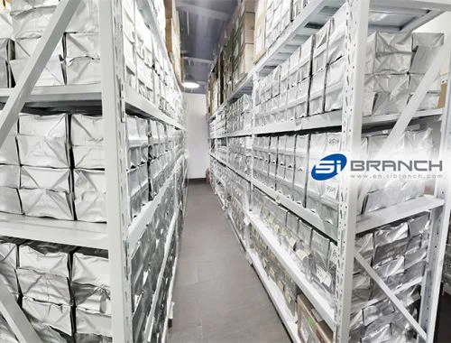
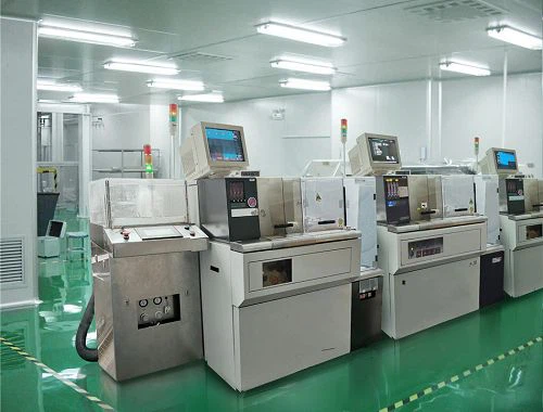
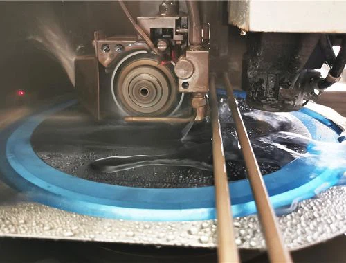
Our vast inventory consists of 1000+ products, ensuring that customers can place orders for as little as one piece. Our self-owned equipments for dicing & backgrinding, and full cooperation in the global industrial chain enable us prompt shipment to ensure customer one-stop satisfaction and convenience.
Our Certificate
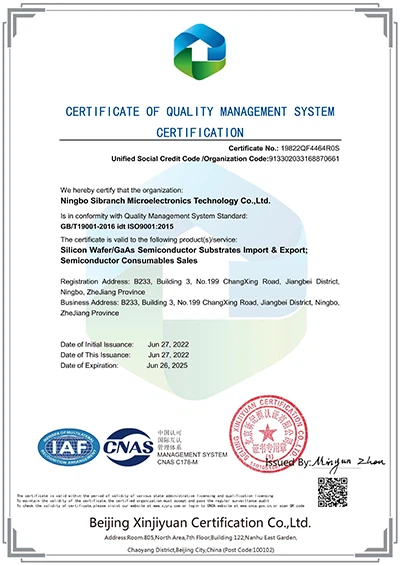
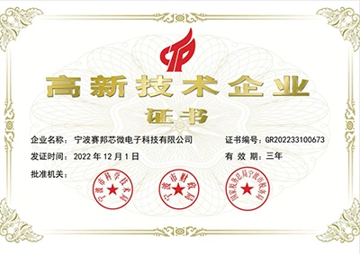
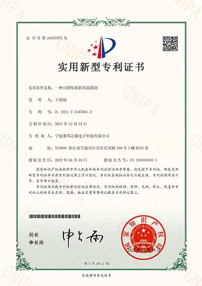
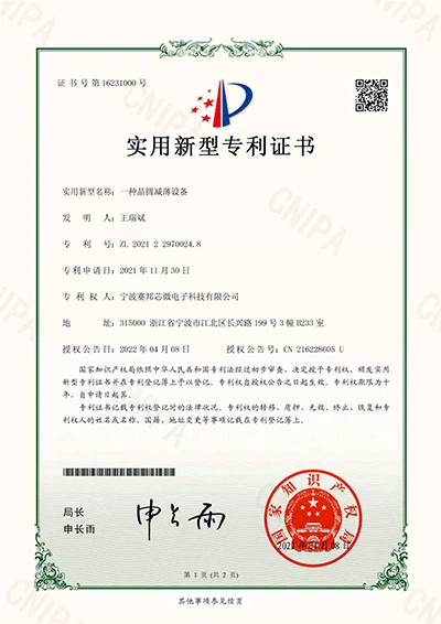
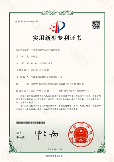
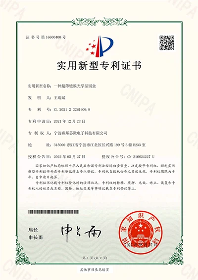
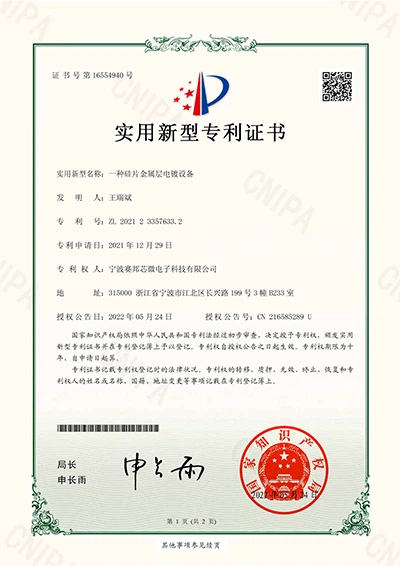
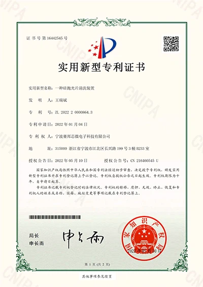
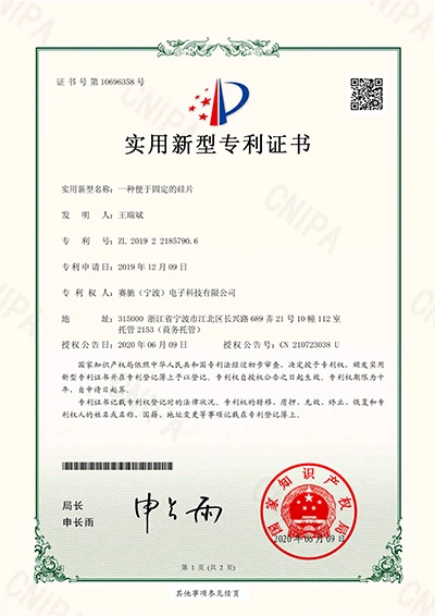
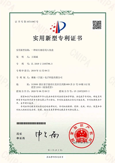
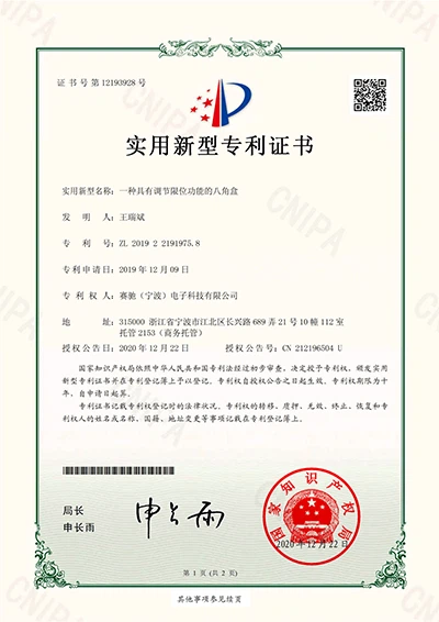
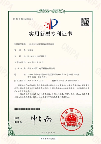
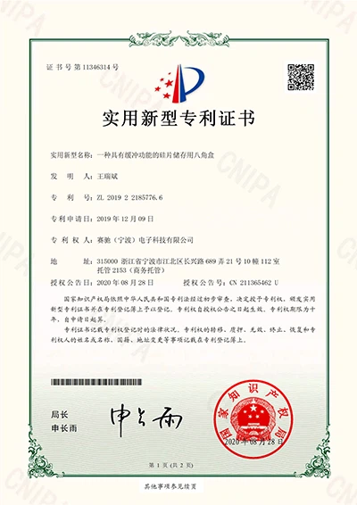
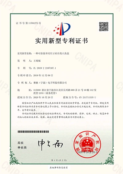
Our company takes pride in the various certifications we have earned, including our patent certificate, ISO9001 certificate, and National High-Tech Enterprise certificate. These certifications represent our dedication to innovation, quality management, and commitment to excellence.
Hot Tags: 300mm silicon wafer, China 300mm silicon wafer manufacturers, suppliers, factory, 450 mm silicon wafer, silicon wafer 300mm, undoped silicon wafer, 12 Inch Silicon Wafer, epitaxial silicon wafer, thick silicon wafers


