


Product Description
Silicon Epitaxial Wafers are highly versatile and can be manufactured in a range of sizes and thicknesses to suit different industry requirements. They are also used in a variety of applications, including integrated circuits, microprocessors, sensors, power electronics, and photovoltaics. The quality of the Silicon Epitaxial Wafers is guaranteed through strict quality control procedures throughout the manufacturing process. This ensures that the wafers are free from defects, impurities and other substances that may impact their performance.
Moreover, the precise and uniform deposition of epitaxial layers on the wafers provide excellent electrical and optical characteristics. During operation, these wafers deliver outstanding performance and dependability. They are designed to withstand extreme temperatures, vibrations, and other harsh conditions, making them ideal for use in a range of environments.
Silicon epitaxy is a process in which an additional monocrystalline silicon layer is deposited on to the polished crystal surface of a silicon wafer. This process makes it possible to select the material properties independently of the polished substrate, and consequently to create wafers that have different properties in the substrate and the epitaxial layer. In many cases this is necessary for the semiconductor component's function.
Sibranch offers silicon epitaxial wafers with diameters to 100~300 mm. While 300 mm EPI wafers are primarily used in highly integrated semiconductor elements (ICs), smaller diameters are also used for power applications. In order to satisfy the various requirements, substrates and epitaxial layers are designed according to customer specifications.
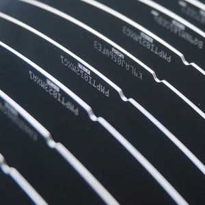
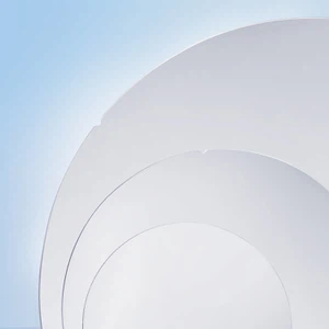
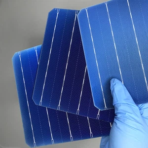
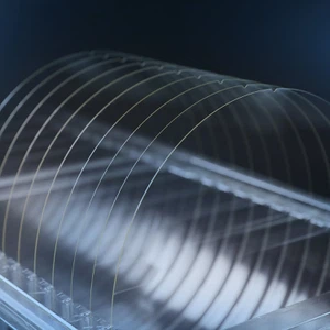
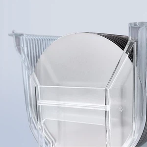
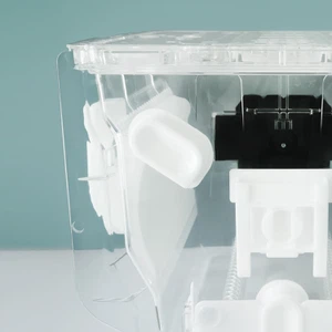
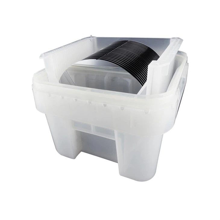
Product Picture


Why Choose Us
Our products are sourced exclusively from the world's top five manufacturers and leading domestic factories. Supported by highly skilled domestic and international technical teams and stringent quality control measures.
Our objective is to provide customers with comprehensive one-on-one support, ensuring smooth channels of communication that are professional, timely, and efficient. We offer a low minimum order quantity and guarantee swift delivery within 24 hours.
Factory Show
Our vast inventory consists of 1000+ products, ensuring that customers can place orders for as little as one piece. Our self-owned equipments for dicing & backgrinding, and full cooperation in the global industrial chain enable us prompt shipment to ensure customer one-stop satisfaction and convenience.


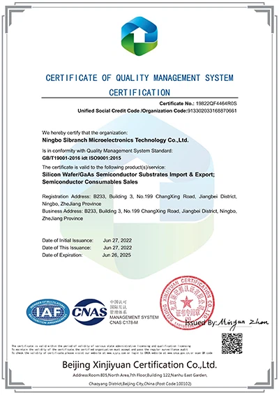
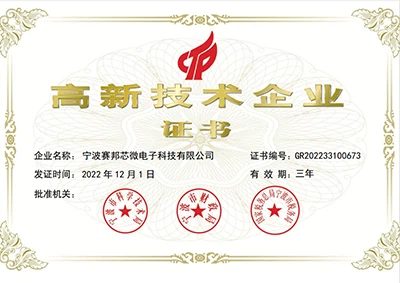
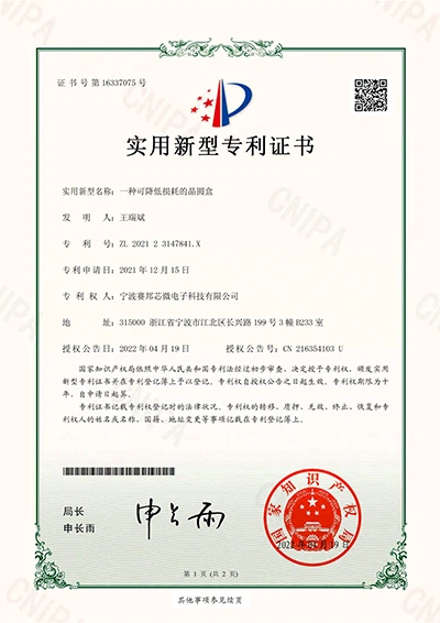
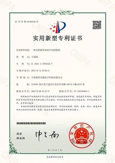
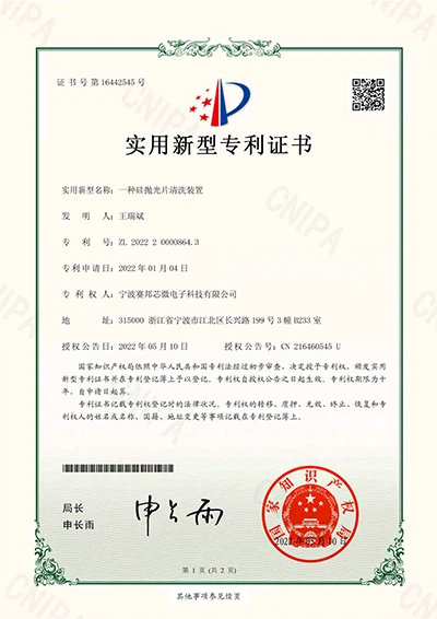
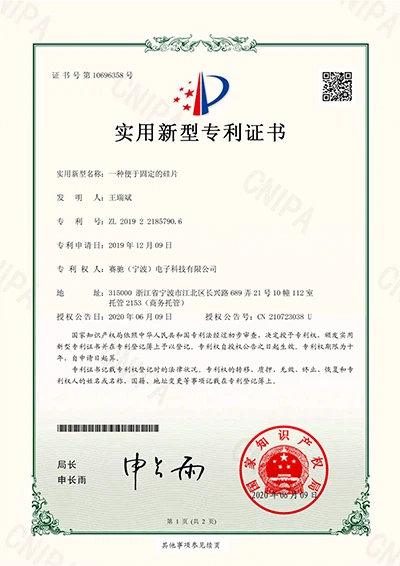
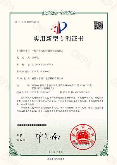
Our Certificate
Our company takes pride in the various certifications we have earned, including our patent certificate, ISO9001 certificate, and National High-Tech Enterprise certificate. These certifications represent our dedication to innovation, quality management, and commitment to excellence.


Hot Tags: silicon epitaxial wafer, China silicon epitaxial wafer manufacturers, suppliers, factory, 12 inch silicon wafers, epitaxial silicon wafer, silicon wafer 300mm, 450 mm silicon wafer, Gold Coated Silicon Wafer, 12 Inch Silicon Wafer


