


Product Description
Sibranch is dedicated to providing high quality polished silicon wafers for a variety of semiconductor and electronics applications. Our 8" (200mm) polished silicon wafers are manufactured to the highest standards, providing superior single crystal monocrystalline material with tightly controlled resistivity and thickness variation specifications. Carefully sliced from single crystal ingots grown using the Czochralski (CZ) method, these wafers are available in single and double side polished styles to ensure excellent thickness uniformity, surface micro-roughness and flatness specifications.

The 200mm silicon wafer is also versatile in its applications, with applications in research and development, as well as in high-volume manufacturing. It can be customized to your exact specifications, with options for thin or thick wafers, polished or unpolished surfaces, and other features based on your specific needs.
|
Growth |
CZ, MCZ, FZ |
|
Grade |
Prime, Test, Dummy, etc. |
|
Diameter |
8 inch / 200mm |
|
Thickness |
200~3000um |
|
Finish |
As cut, lapped, etched, SSP, DSP, etc. |
|
Orientation |
(100) (111) (110) (531) (553) etc. |
|
Off cut |
Up to 4 deg |
|
Type/Dopant |
P/B, N/Phos, N/As, N/Sb, Intrinsic |
|
Resistivity |
CZ/MCZ: From 0.001 to 1000 ohm-cm |
|
FZ: Up to 20k ohm-cm |
|
|
Thin films |
* PVD: Al, Cu, Au, Cr, Si, Ni, Fe, Mo. etc, Coating thicknesses up to 20, 000 Å / ± 5 % |
|
* LPCVD/PECVD: Oxide, Nitride, SiC, etc, Coating thicknesses up to 200, 000 Å / ± 3 % |
|
|
* Silicon epitaxial wafers and epitaxial services (SOS, GaN, GOI etc). |
|
|
Processes |
DSP, ultra thin, ultra flat, etc. |
|
Downsizing, back grinding, dicing , etc. |
|
|
MEMS |
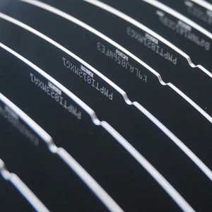
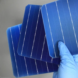
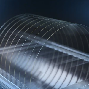
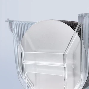
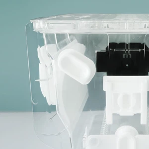
Product Picture

What are 200 mm silicon wafers used for?
200 mm silicon wafers are commonly used to manufacture a variety of electronic devices, including integrated circuits (ICs), microelectromechanical systems (MEMS), and optoelectronic devices.
200 mm wafers are between the smaller 150 mm wafers and the larger 300 mm wafers. They are a more economical alternative to larger wafers while still providing a relatively large surface area for device manufacturing. 200 mm wafers are also compatible with a variety of manufacturing processes and equipment, making them a versatile choice for many applications.
Some examples of devices that can be manufactured on 200 mm wafers include:
Integrated Circuits: 200 mm wafers are used to manufacture a variety of integrated circuits, including microprocessors, memory chips, and other complex circuits.
MEMS Devices: 200 mm wafers are used to manufacture microelectromechanical systems (MEMS), which are tiny devices that combine mechanical and electronic components on a single substrate. Examples of MEMS devices include sensors, actuators, and microfluidic devices.
Optoelectronic devices: 200 mm wafers are also used to manufacture optoelectronic devices such as lasers, light emitting diodes (LEDs), and photodetectors.
Frequently Asked Questions about 200mm and 300mm Wafers
What are the main differences between 200mm and 300mm wafers?
The main difference is that 300mm wafers are larger, with more than 2x the surface area per wafer compared to 200mm. This allows more chips to be produced per wafer, which reduces costs. However, 300mm requires more advanced expertise and higher startup costs.
Why are some chips still produced on 200mm wafers?
Many chips do not require advanced process nodes below 10nm. Mature nodes on 200mm are sufficient for applications such as RF, MEMS, automotive ICs, etc., while also providing high yield and utilization of existing assets.
What process nodes do 300mm wafers support?
300mm wafers are used for leading-edge nodes below 10nm, such as 5nm, 3nm, etc. The world's largest foundries are focused on expanding capacity on 300mm wafers to enable manufacturing below 10nm.
Can you convert a 200mm fab to process 300mm wafers?
No. Moving to 300mm requires a completely new fab with larger, tailored equipment and facilities. The upfront capital and R&D costs for a 300mm start-up exceed billions of dollars.
Which wafer size is expected to grow faster?
Both sizes will see strong growth. 300mm remains a leader in the leading edge before 3nm, while 200mm capacity is also expected to expand, especially in analog, MEMS, and trailing-edge nodes.
What are the factors driving the increase in new fabs for both wafer sizes?
In particular, the growing demand for 5G, AI, high-performance computing, cloud, and edge data centers is driving investments in expanding 200mm and 300mm capacity for different types of chips.
Why Choose Us
Our products are sourced exclusively from the world's top five manufacturers and leading domestic factories. Supported by highly skilled domestic and international technical teams and stringent quality control measures.
Our objective is to provide customers with comprehensive one-on-one support, ensuring smooth channels of communication that are professional, timely, and efficient. We offer a low minimum order quantity and guarantee swift delivery within 24 hours.
Factory Show
Our vast inventory consists of 1000+ products, ensuring that customers can place orders for as little as one piece. Our self-owned equipments for dicing & backgrinding, and full cooperation in the global industrial chain enable us prompt shipment to ensure customer one-stop satisfaction and convenience.


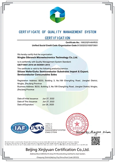
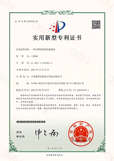
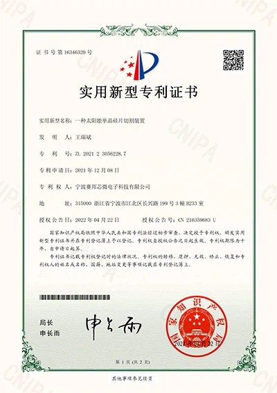
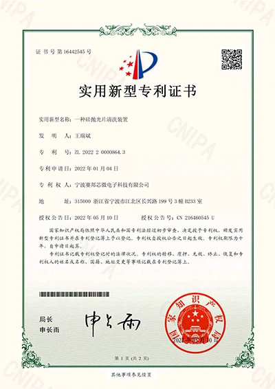
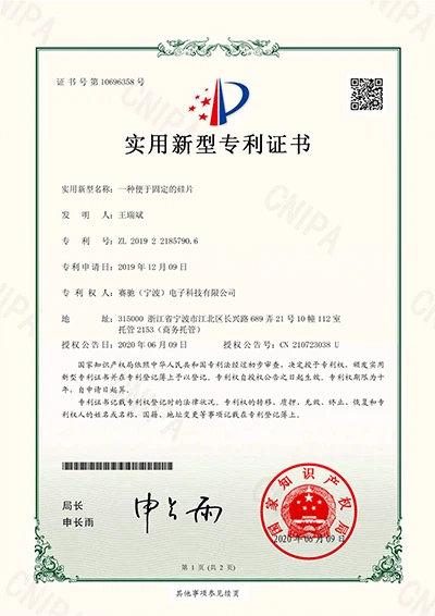
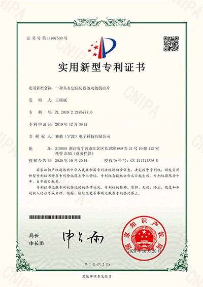
Our Certificate
Our company takes pride in the various certifications we have earned, including our patent certificate, ISO9001 certificate, and National High-Tech Enterprise certificate. These certifications represent our dedication to innovation, quality management, and commitment to excellence.


Hot Tags: 200mm silicon wafer, China 200mm silicon wafer manufacturers, suppliers, factory, 450 mm silicon wafer, epitaxial silicon wafer, thick silicon wafers, Gold Coated Silicon Wafer, float zone silicon wafer, 12 Inch Silicon Wafer


