


Ningbo Sibranch Microelectronics Technology Co.,Ltd.:Your Trustworthy 300mm Silicon Wafer Manufacturer!
Founded in 2006 by material science and engineering scientist in Ningbo, China, Sibranch Microelectronics aims to provide semiconductor wafer and service all over the world. Our main products include standard silicon wafers SSP (single side polished), DSP (Double side polished), test silicon wafers and prime silicon wafers, SOI (Silicon on Insulator) wafer and coin roll wafers with diameter up to 12 inch, CZ/MCZ/FZ/NTD, almost any orientation, off cut, high and low resistivity, ultra-flat, ultra-thin, thick wafers etc.
Leading Service
We are committed to constantly innovating our products to provide foreign customers with a large number of high-quality products to exceed customer satisfaction. We can also provide customized services according to customers' requirements such as size, color, appearance, etc. We can provide the most favorable price and high-quality products.
Quality Guaranteed
We have been continuously researching and innovating to meet the needs of different customers. At the same time, we always adhere to strict quality control to ensure that the quality of every product meets international standards.
Wide Sales Countries
We focus on sales in overseas markets. Our products are exported to Europe, America, Southeast Asia, the Middle East and other regions, and are well received by customers around the world.
Various Types of Products
Our company offers customized silicon wafer processing services tailored to meet the specific needs of our clients. These include Si Wafer BackGrinding, Dicing, DownSizing, Edge Grinding, as well as MEMS among others. We strive to deliver bespoke solutions that exceed expectations and ensure customer satisfaction.
Product Types

CZ Silicon Wafers are cut from single crystal silicon ingots pulled using the Czochralski CZ growth method, which is most widely used in the electronics industry to grow silicon crystals from large cylindrical silicon ingots used to manufacture semiconductor devices. In this process, an elongated crystalline silicon seed with precise orientation tolerance is introduced into a silicon molten pool with precisely controlled temperature. The seed crystal is slowly pulled upward from the melt at a strictly controlled rate, and crystal solidification of the liquid phase atoms occurs at the interface. During this pulling process, the seed crystal and the crucible rotate in opposite directions, forming a large single crystal silicon with a perfect crystal structure of the seed.

Silicon oxide wafer is an advanced and essential material used in various high-tech industries and applications. It is a high-purity crystalline substance produced by processing high-quality silicon materials, making it an ideal substrate for many different types of electronic and photonic applications.

Dummy wafers (also called test wafers) are wafers mainly used for experiment and test and are different from general wafers for product. Accordingly, reclaimed wafers are mostly applied as dummy wafers (test wafers).

Gold-coated silicon wafers, and gold-coated silicon chips are used extensively as substrates for analytical characterization of materials. For example, materials deposited onto gold-coated wafers can be analyzed via ellipsometry, Raman spectroscopy or infrared (IR) spectroscopy due to the high-reflectivity and favorable optical properties of gold.

Silicon Epitaxial Wafers are highly versatile and can be manufactured in a range of sizes and thicknesses to suit different industry requirements. They are also used in a variety of applications, including integrated circuits, microprocessors, sensors, power electronics, and photovoltaics.

Manufactured using the latest technology and is designed to offer unparalleled reliability and consistency in performance. Thermal Oxide Dry and Wet is an essential tool for semiconductor manufacturers worldwide as it provides an efficient way to produce high-quality wafers that meet all the demanding requirements of the industry.

This wafer has a diameter of 300 millimeters, making it larger than traditional wafer sizes. This larger size makes it more cost-effective and efficient, allowing for greater production output without sacrificing quality.

The 100mm silicon wafer is a high-quality product that is widely used in the electronics and semiconductor industries. This wafer is designed to provide optimal performance, precision, and reliability that are essential in the manufacturing of semiconductor devices.

The 200mm silicon wafer is also versatile in its applications, with applications in research and development, as well as in high-volume manufacturing. It can be customized to your exact specifications, with options for thin or thick wafers, polished or unpolished surfaces, and other features based on your specific needs.
Wha
t is Thermal Oxide Silicon Wafer
Thermal Oxide Silicon Wafers are silicon wafers that have a layer of silicon dioxide (SiO₂) formed on their surface. The thermal oxide layer (Si+SiO₂) is grown on a bare silicon wafer at elevated temperatures in the presence of an oxidant through the thermal oxidation process. It is typically grown in a horizontal tube furnace at temperatures ranging from 900°C to 1200°C, using either "Wet" or "Dry" growth methods.
Thermal oxide is a "grown" oxide layer. Compared to CVD-deposited oxide layers, it provides an excellent dielectric layer as an insulator with higher uniformity and greater dielectric strength. For most silicon-based devices, the thermal oxide layer plays a critical role in passivating the silicon surface, acting as doping barriers and surface dielectrics.
Types of Thermal Oxide Silicon Wafers
Wet Thermal Oxide on Both Sides of Wafer Film thickness
500Å – 10µm on both sides Film thickness tolerance: Target ±5% Film stress: –320±50 MPa Compressive
01
Wet Thermal Oxide on Single Side of Wafer Film thickness
500Å – 10,000Å on single side Film thickness tolerance: Target ±5% Film stress: -320±50 MPa Compressive
02
Dry Thermal Oxide on Both Sides of Wafer Film thickness
100Å – 3,000Å on both sides Film thickness tolerance: Target ±5% Film stress: –320±50 MPa Compressive
03
Dry Thermal Oxide on Single Side of Wafer Film thickness
100Å – 3,000Å on single side Film thickness tolerance: Target ±5% Film stress: –320±50 MPa Compressive
04
Dry Chlorinated Thermal Oxide with Forming Gas Anneal Film thickness
100Å – 3,000Å on both sides Film thickness tolerance: Target ±5% Film stress: –320±50 MPa Compressive Sides Process: Both Sides
05
Manufacturing Process of Thermal Oxide Silicon Wafer
Thermal oxidation of silicon begins by placing the silicon wafers on a quartz rack, commonly known as a boat, which is then heated in a quartz thermal oxidation furnace. Under standard pressure, the furnace temperature is typically maintained between 950°C and 1,250°C. A control system is required to keep the temperature within approximately ±5°C of the setpoint.
Depending on the type of oxidation being performed, either oxygen or steam is introduced into the furnace. Oxygen from these gases diffuses from the substrate surface through the existing oxide layer to reach the silicon interface, where it reacts to form new oxide. The composition and depth of the oxidation layer can be precisely controlled by adjusting parameters such as time, temperature, pressure, and gas concentration.
Higher temperatures increase the oxidation rate but also promote diffusion of impurities and movement of junctions between the silicon and oxide layers. These effects are particularly undesirable when the oxidation process requires multiple steps, as is the case with complex integrated circuits. Lower temperatures produce higher quality oxide layers but increase growth time.
A common solution to this trade-off is to heat the wafers at relatively low temperatures under high pressure to reduce growth time. All other factors being equal, an increase of one standard atmosphere (atm) decreases the required temperature by approximately 20°C. Industrial applications often use up to 25 atm of pressure with temperatures between 700°C and 900°C.
The oxide growth rate is initially very fast but slows as oxygen must diffuse through a thicker oxide layer to reach the silicon substrate. After oxidation is complete, approximately 46% of the final oxide thickness penetrates below the original substrate surface, leaving 54% of the oxide layer above the original surface.
Frequently Asked Questions
Q: What is thermal oxide on a silicon wafer?
A: Thermal oxidation is the process of exposing a silicon wafer to a combination of oxidizing agents and heat to form a layer of silicon dioxide (SiO₂). This layer is most commonly formed using oxygen and/or hydrogen gas, although halogen gases can also be used.
Q: What are the two main types of thermal oxidation?
A: The two primary types are dry thermal oxidation (using oxygen) and wet thermal oxidation (using water vapor/steam). Oxygen or water molecules react with the silicon surface, gradually forming a thin oxide layer.
Q: What happens when a silicon wafer is placed in a high-temperature furnace with oxygen or steam?
A: Thermal oxidation occurs as the silicon wafer reacts with oxygen or steam at high temperature to form SiO₂. Thermally grown oxides generally exhibit superior dielectric properties compared to deposited oxides. While the oxide structure is amorphous, it is strongly bonded to the underlying silicon surface.
Q: What is the difference between wet and dry thermal oxide?
A: The refractive index of wet and dry thermal oxide is not measurably different. However, dry thermal oxide exhibits lower leakage current and higher dielectric strength than wet oxide. At very low thicknesses (less than 100nm), dry oxide thickness can be controlled more precisely because it grows slower than wet oxide.
Q: What is the thickness of the native oxide layer on a silicon wafer?
A: A thin native oxide layer (approximately 1.5 nm or 15 Å [angstroms]) forms spontaneously on the surface of a silicon wafer whenever the wafer is exposed to air under ambient conditions.
Q: Why is thermal oxidation preferred for growing SiO₂ as gate oxide?
A: For the highest quality oxides such as gate oxides, dry thermal oxidation is preferred. Advantages include a slower oxidation rate, better control of oxide thickness for thin layers, and high breakdown field strength.
Q: How do you remove an oxide layer from silicon?
A: Silicon dioxide layers can be removed from silicon substrates using various methods. One common approach involves soaking the wafer in an etching solution to remove most of the silicon oxide layer, followed by rinsing the wafer surface to remove residual silicon oxide.
Q: What is the purpose of using a thermally grown oxide layer as a starting layer in semiconductor fabrication?
A: Thermal oxidation of silicon is a common fabrication step for MEMS and semiconductor devices. The process helps improve silicon wafer surface quality by removing unwanted particles and produces thin films with high electrical strength and purity.
Q: How much of the original silicon surface is consumed during thermal oxide growth?
A: Silicon dioxide growth occurs with approximately 54% of the final oxide above the original silicon surface and 46% below, as silicon is consumed during the reaction. The wet oxidation rate is faster than the dry oxidation process. Therefore, dry oxidation is suitable for forming thin oxide layers to passivate the silicon surface.
Q: What is dry oxidation of a silicon wafer?
A: Dry oxidation typically uses high-purity oxygen gas to react with silicon. Nitrogen gas is commonly used as a purge gas during system idle, temperature ramping, wafer loading, and chamber purging steps because nitrogen does not react with silicon at typical processing temperatures.
Q: What type of silicon substrate is used for oxidation?
A: Single crystal <100> silicon or silicon with a slight miscut (<100>±0.5°) provides the best results. Moderate doping levels (1-100 Ωcm resistivity) are preferred. Larger diameters up to 300mm are common for modern thermal oxidation processes.
Q: Why is surface condition so important?
A: An organic-free surface with minimal roughness enables uniform oxidation and minimizes defects in the oxide layer. Cleaning procedures aim to remove organic contamination and particles down to <100/cm² level.
Q: What causes variation in oxidation rate?
A: The primary drivers are temperature and oxidant ambient. However, parameters such as doping concentration, defect density, crystal orientation, and surface roughness also impact diffusion rates, which govern oxidation kinetics.
Q: What problems can arise from non-uniform oxidation?
A: Spatial differences in thickness or composition degrade device performance and yield. Uniformity targets are generally <±1% variation across a wafer.
Q: How pure must the silicon substrate be?
A: High purity with minimal metallic or crystallographic contamination is essential for gate dielectric quality. Silicon for advanced nodes may require purity levels beyond 11 nines (99.999999999%).
Q: Can silicon oxide replace silicon substrates in semiconductor devices?
A: No. Silicon oxide serves an isolation and dielectric function, but active devices like transistors require an underlying semiconductor substrate such as silicon for functionality. Only silicon itself enables efficient switching behavior.
Q: How much silicon is consumed during oxidation?
A: Approximately 44-46% of the final oxide thickness results from consumption of the silicon wafer itself. The remainder comes from the oxygen source. This ratio contributes to determining final oxide purity.
Why Choose Us
Our products are sourced exclusively from the world's top five manufacturers and leading domestic factories. Supported by highly skilled domestic and international technical teams and stringent quality control measures.
Our objective is to provide customers with comprehensive one-on-one support, ensuring smooth channels of communication that are professional, timely, and efficient. We offer a low minimum order quantity and guarantee swift delivery within 24 hours.
Factory Show
Our vast inventory consists of 1000+ products, ensuring that customers can place orders for as little as one piece. Our self-owned equipments for dicing & backgrinding, and full cooperation in the global industrial chain enable us prompt shipment to ensure customer one-stop satisfaction and convenience.


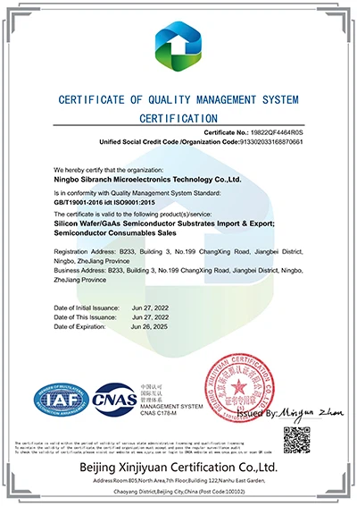
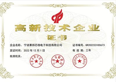
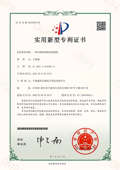
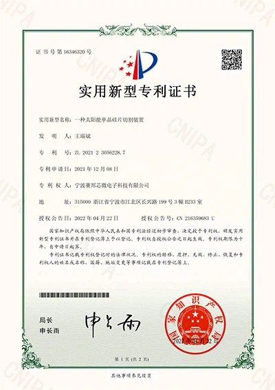
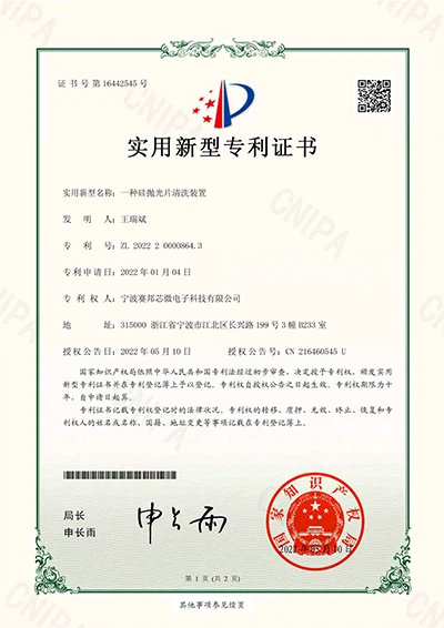
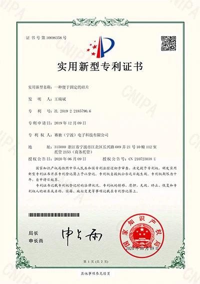
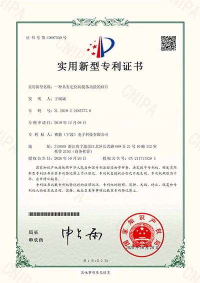
Our Certificate
Our company takes pride in the various certifications we have earned, including our patent certificate, ISO9001 certificate, and National High-Tech Enterprise certificate. These certifications represent our dedication to innovation, quality management, and commitment to excellence.


Hot Tags: thermal oxide silicon wafer, China thermal oxide silicon wafer manufacturers, suppliers, factory, silicon wafer 300mm, undoped silicon wafer, float zone silicon wafer, epitaxial silicon wafer, 12 Inch Silicon Wafer, Gold Coated Silicon Wafer


