






Product Overview
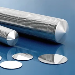
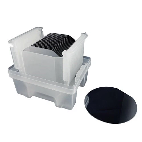
Sibranch Microelectronics offers high-precision 100mm (4-inch) silicon wafers manufactured with CZ, MCZ and FZ growth methods. Our wafers are engineered to meet the strict requirements of the semiconductor, MEMS, sensor, power-device and research-institute markets, delivering consistent geometry, tightly controlled resistivity and reliable surface quality.
Backed by sourcing from the world's leading silicon manufacturers and supported by our in-house processing capabilities (dicing, back-grinding, polishing, coating), we provide a one-stop supply solution from a single piece for prototyping up to volume production - typically shipped within 24 hours from stock.
Technical Specifications
|
Parameter |
Specification |
|
Diameter |
100 mm (4 inch) |
|
Growth Method |
CZ (Czochralski), MCZ (Magnetic CZ), FZ (Float Zone) |
|
Grade |
Prime, Test, Mechanical / Dummy, Reclaim |
|
Thickness |
50 – 3000 μm (customizable, including ultra-thin <100 μm) |
|
Surface Finish |
As-cut, Lapped, Etched, SSP (Single-Side Polished), DSP (Double-Side Polished) |
|
Crystal Orientation |
(100), (111), (110), (211), (311), (511), (531), etc. |
|
Off-cut Angle |
0° – 7° (customizable on request) |
|
Type / Dopant |
P-type: B | N-type: Phos, As, Sb | Intrinsic (undoped) |
|
Resistivity (CZ / MCZ) |
0.001 – 1000 Ω·cm |
|
Resistivity (FZ) |
Up to 20,000 Ω·cm (high-resistivity) |
|
TTV / Bow / Warp |
TTV ≤ 5 μm, Bow / Warp ≤ 30 μm (Prime grade, typical) |
|
Edge Profile |
Rounded / Chamfered (R-type), per SEMI standard |
|
Packaging |
Class 100 / Class 10 cleanroom packaging, single-wafer or cassette |
Thin Films, Coatings & Epitaxial Services
PVD (Physical Vapor Deposition):
- Metals: Al, Cu, Au, Cr, Ni, Fe, Mo, Si, etc.
- Coating thickness up to 20,000 Å, tolerance ±5%.
LPCVD / PECVD:
- Dielectrics: SiO₂ (Oxide), Si₃N₄ (Nitride), SiC, etc.
- Coating thickness up to 200,000 Å, tolerance ±3%.
Epitaxial Wafers:
- Si-Epi on Si, SOS (Silicon-on-Sapphire), GaN-on-Si, GOI (Germanium-on-Insulator), and other custom epi services.
Wafer Processing Services
- Double-Side Polishing (DSP) - high-flatness surface for advanced lithography.
- Ultra-thin grinding - final thickness down to <50 μm.
- Ultra-flat processing - tight TTV / Bow / Warp control.
- Dicing / Down-sizing - customized chips and small wafers from standard substrates.
- Back-grinding - controlled wafer thinning for packaging.
- MEMS-grade processing - DSP + ultra-flat + tight tolerance.
Typical Applications
- Discrete devices and power semiconductors (Diodes, MOSFETs, IGBTs)
- MEMS sensors (pressure, accelerometer, gyroscope, microphone)
- Optoelectronics and photonic devices
- RF and high-frequency components
- Solar cell research and pilot lines
- University and R&D institute test vehicles
- IC fabrication processes and equipment qualification
Why Choose Sibranch
- Premium Supply Chain: Wafers sourced exclusively from the world's top-five silicon manufacturers and leading domestic fabs.
- Professional Technical Support: Experienced engineering team in China and overseas, providing one-on-one technical consultation.
- Flexible MOQ: Order from just 1 piece for R&D samples, up to mass-production volumes.
- Fast Delivery: Standard stock items shipped within 24 hours; customized orders with industry-leading lead times.
- In-house Capability: Self-owned equipment for dicing, back-grinding and downsizing - full control over quality and schedule.
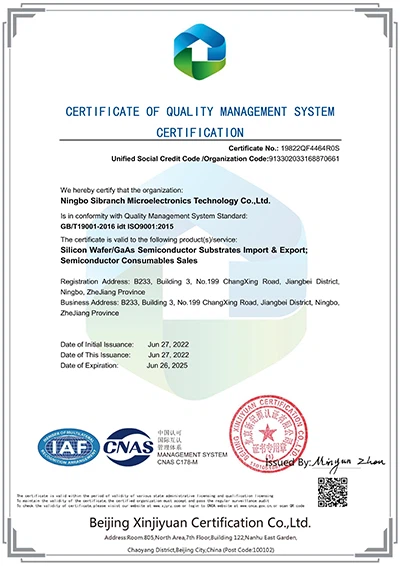
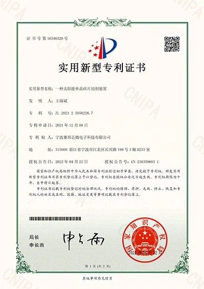
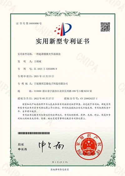
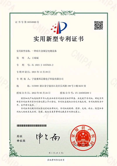
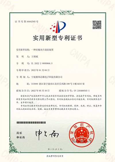
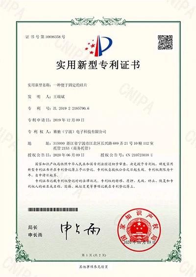
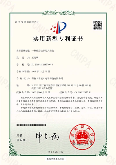
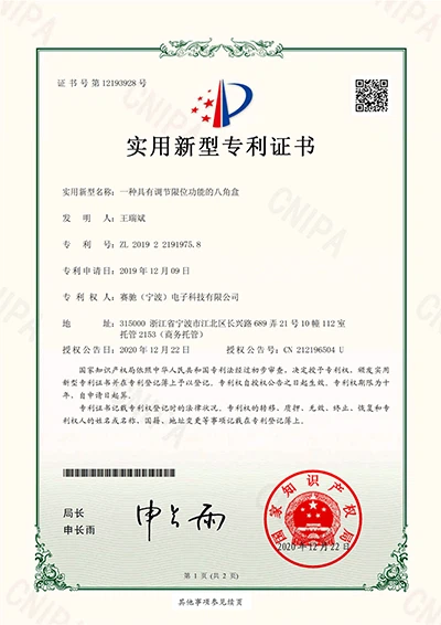
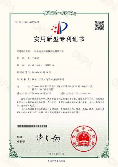
- Quality Assurance: ISO 9001 certified, National High-Tech Enterprise, with patent certifications and strict incoming/outgoing QC.
Certifications
- ISO 9001 Quality Management System
- National High-Tech Enterprise
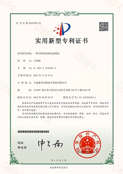
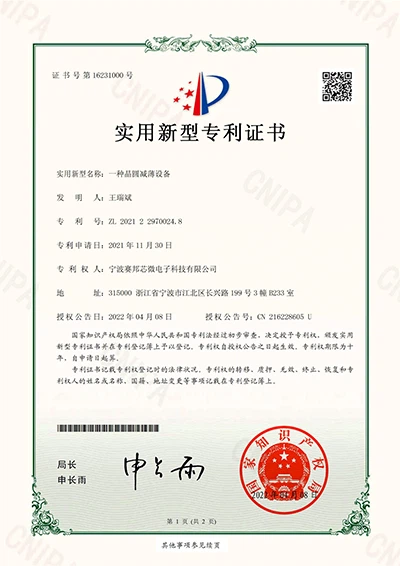
- Multiple invention and utility-model patents
Contact Us
- Company: Ningbo Sibranch Microelectronics Technology Co., Ltd.
- Website: www.sibranchwafer.com | www.sibranch.com
- Inquiry: Please contact our sales team for datasheets, samples and customized quotations.
Product Picture

Why Choose Us
Our products are sourced exclusively from the world's top five manufacturers and leading domestic factories. Supported by highly skilled domestic and international technical teams and stringent quality control measures.
Our objective is to provide customers with comprehensive one-on-one support, ensuring smooth channels of communication that are professional, timely, and efficient. We offer a low minimum order quantity and guarantee swift delivery within 24 hours.
Factory Show
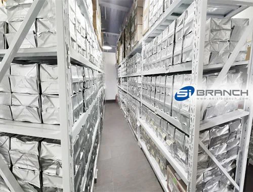
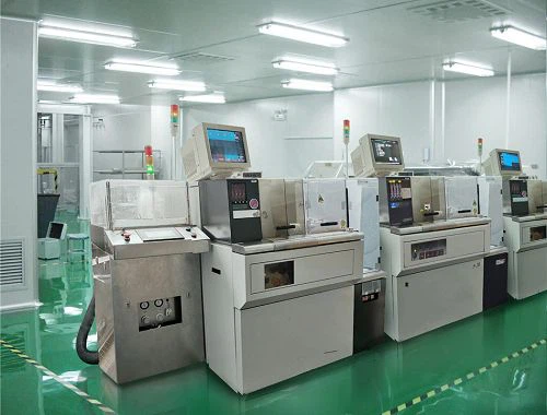
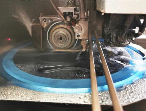
Our vast inventory consists of 1000+ products, ensuring that customers can place orders for as little as one piece. Our self-owned equipments for dicing & backgrinding, and full cooperation in the global industrial chain enable us prompt shipment to ensure customer one-stop satisfaction and convenience.
Our Certificate
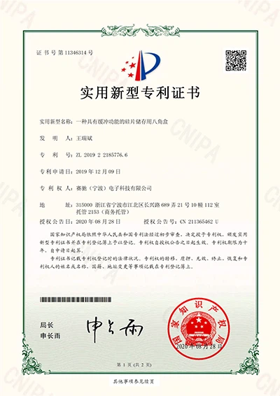
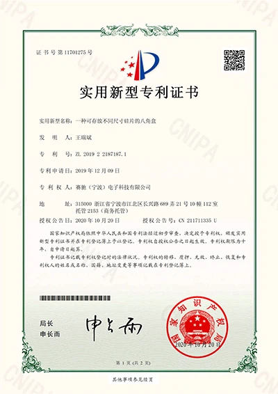
Our company takes pride in the various certifications we have earned, including our patent certificate, ISO9001 certificate, and National High-Tech Enterprise certificate. These certifications represent our dedication to innovation, quality management, and commitment to excellence.

Hot Tags: 100mm silicon wafer, China 100mm silicon wafer manufacturers, suppliers, factory, float zone silicon wafer, Gold Coated Silicon Wafer, thick silicon wafers, epitaxial silicon wafer, silicon wafer 300mm, undoped silicon wafer


