


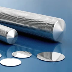




Silicon Carbide Wafer
Ningbo Sibranch Microelectronics Technology Co.,Ltd.:Your Trustworthy Silicon Carbide Wafer Manufacturer!
Founded in 2006 by material science and engineering scientist in Ningbo, China, Sibranch Microelectronics aims to provide semiconductor wafer and service all over the world. Our main products including standard silicon wafers SSP (single side polished), DSP (Double side polished), test silicon wafers and prime silicon wafers, SOI (Silicon on Insulator) wafer and coinroll wafers with diameter up to 12 inch, CZ/MCZ/FZ/NTD, almost any orientation, off cut, high and low resistivity, ultra flat, ultra thin, thick wafers etc.
Leading Service
We are committed to constantly innovating our products to provide foreign customers with a large number of high-quality products to exceed customer satisfaction. We can also provide customized services according to customers' requirements such as size,color,appearance,etc.We can provide the most favorable price and high-quality products.
Quality Guaranteed
We have been continuously researching and innovating to meet the needs of different customers. At the same time, we always adhere to strict quality control to ensure that the quality of every product meets international standards.
Wide Sales Countries
We focus on sales in overseas markets. Our products are exported to Europe, America,Southeast Asia,the Middle East and other regions, and are well received by customers around the world.
Various Types of Products
Our company offers customized silicon wafer processing services tailored to meet the specific needs of our clients. These include Si Wafer BackGrinding、Dicing,DownSizing、Edge Grinding, as well as MEMS among others. We strive to deliver bespoke solutions that exceed expectations and ensure customer satisfaction.


What is Silicon Carbide Wafer
A silicon carbide wafer is a crystalline material that is made by etching the crystal. It is typically thin enough to be used for power semiconductor devices. The other type is a type of insulator. The temperature range is extremely important for electrical and magnetic fields in power semiconductors.
Bandgap and Thermal Conductivity
With its wide bandgap, silicon carbide wafers can withstand voltages that are up to ten times higher than silicon, which has a breakdown voltage of around 600V. Silicon (Si), a semiconductor that’s long been the material of choice for the wafers used in integrated circuits (ICs) and photovoltaics, has a bandgap of 1.12 eV. Gallium arsenide (GaAs), a semiconductor used in solar cells, has a bandgap of 1.42 eV. By contrast, silicon carbide has a bandgap of 3.26 eV. SiC’s wider bandgap also support faster, more efficient switching and smaller, thinner devices. In addition, silicon carbide’s higher thermal conductivity allows for the more efficient transportation of heat and can reduce or eliminate the need for heat sinks in electronic designs.
Thermal Shock Resistance
With its high thermal conductivity and low thermal expansion, silicone carbide also provides superior resistance to thermal shock, a transient mechanical load caused by a rapid change of temperature. Often, thermal shock occurs when an extreme temperature gradient reaches some but not all of an object. Because of this difference in temperature, parts of the object expand and contract at different rates, which can lead to fracture. Compared to most semiconductor materials, SiC has a low thermal conductivity (3.8 W/m.K minimum) and a high thermal expansion (7.9 to 11 10-6/K).
Physical, Chemical and Electrical Durability
Silicon carbide’s physical durability is demonstrated by its use in non-electronic applications such as the plates in bulletproof vests. With regard to temperature durability, SiC will not sublimate into a vapor phase until around 2700°C, which is significantly higher than the melting point of iron (around 1500°C). SiC is also chemically inert and can resist very aggressive chemicals such as alkalis and molten salts, even at high temperatures up to 800°C. With its high energy bandgap, SiC is extremely resistant to high levels of electromagnetic disturbances and the damaging effects of radiation.
Versatility
Silicone carbide’s superior properties makes it good choice for EV power electronics. Applications include on-board DC/DC converters, off-board DC fast chargers, on-board battery chargers, EV powertrains, and automotive lighting for LEDs. In addition to high-temperature resistance, silicon carbide provides the low power consumption, rigidity, and support for smaller, thinner designs that EV power electronics need. With their greater power densities and higher amounts of heat, 5G electronics are also using SiC wafers.
Hardness
There are numerous advantages to using silicon carbide over more traditional silicon substrates. One of the major advantages is its hardness. This gives the material many advantages, in high speed, high temperature and/or high voltage applications. Silicon carbide wafers have high thermal conductivity, which means they can transfer heat from one point to another well. This improves its electrical conductivity and ultimately miniaturization, one of the common goals of switching to SiC wafers.
Thermal capabilities
Silicon carbide substrates also have a low coefficient for thermal expansion. Thermal expansion is the amount and direction a material expands or contracts as it heats up or cools down. The most common explanation is ice, although it behaves opposite of most metals, expanding as it cools and shrinking as it heats up. Silicon carbide’s low coefficient for thermal expansion means that it does not change significantly in size or shape as it is heated up or cooled down, which makes it perfect for fitting into small devices and packing more transistors onto a single chip. Another major advantage of these substrates is their high resistance to thermal shock. This means they have the ability to change temperatures rapidly without breaking or cracking. This creates a clear advantage when fabricating devices as it is another toughness characteristic that improves the lifetime and performance of silicon carbide in comparison to traditional bulk silicon. On top of its thermal capabilities, it is a very durable substrate and does not react with acids, alkalis or molten salts at temperatures up to 800°C. This gives these substrates versatility in their applications and further assists their ability to out perform bulk silicon in many applications. Its strength at high temperatures also allows it to safely operate at temperatures over 1600°C. This makes it a suitable substrate for virtually any high temperature application.
Larger Wafers, Greater Efficiency
The availability of SiC wafers with larger diameters, reaching up to 150mm and even 200mm, is a game-changer. These larger wafers allow for increased device integration on a single chip, leading to higher production throughput and ultimately reduced manufacturing costs per unit area.
Taming Defects, Refining Quality
The relentless pursuit of reducing defects and improving crystal quality has spurred the development of advanced growth techniques. Techniques like Continuous Feed Physical Vapor Transport (CF-PVT) and refined High-Temperature Chemical Vapor Deposition (HTCVD) minimize defect densities and pave the way for exceptional SiC crystals.
State-of-the-Art Characteristics
Leading manufacturers are delivering SiC wafers with truly impressive characteristics. Low defect densities (often less than 10 micropipes per square centimeter) and high carrier lifetimes are hallmarks of these advanced wafers. This translates to the fabrication of high-performance SiC devices with superior efficiency and reliability.
Epitaxial Growth Takes Center Stage
Significant advancements in epitaxial growth techniques are contributing to the overall quality of SiC wafers. Cutting-edge methods like Chloride-Based Chemical Vapor Deposition (CVD) and Trichlorosilane (TCS) CVD offer unparalleled control over doping profiles, layer thickness, and defect densities within the epitaxial SiC layers.
Doping with Precision
Doping, the process of introducing impurities to control the electrical properties of SiC wafers, has become an art form. Techniques like ion implantation and in-situ doping during epitaxial growth have been meticulously refined, allowing for precise control over dopant concentrations and activation. Common dopants include nitrogen for n-type (electron-rich) and aluminum or boron for p-type (hole-rich) conductivity.
Seeing the Unseen
Advanced Characterization: The relentless pursuit of perfection extends to characterization techniques. Advanced methods like X-ray topography, photoluminescence mapping, and scanning electron microscopy (SEM) are used to not only identify defects but also analyze them in detail. This continuous monitoring allows manufacturers to refine their processes and steadily improve wafer quality, ultimately leading to even better device performance.
First acetone and ethanol are made into mixed solution according to the ratio of 3: 1, are heated to 50 ℃. In cleaning process, place the mixed solution of 3 glasss of above-mentioned heat, silicon carbide wafer soaks 3 minutes in every glass of solution, cleans successively. After every cleaning 6 wafer, first glass of more muddy solution is changed to its excess-three cup prerequisite successively, the clean mixed solution that last glass renews. Often washing afterwards 3 silicon carbide wafers uses the same method and uses one glass of mixed solution instead. In cleaning process, can determine the ratio of using instead according to the number of wax and the Turbidity of solution, to reach best cleaning performance and most cost-saving benefit.
Silicon carbide wafer after acetone cleans should reach following effect: surperficial without visible pollutant in the lower observation of turning off the light by force. Use afterwards deionized water rinsing silicon carbide wafer positive and negative each 30 seconds, in the supersonic wave cleaning machine that is 700kHz in frequency, use ethanolic solution cleaning sic wafer 5 minutes, to remove the paraffin of remained on surface and to reduce other organic pollution. This step is further removed the organic pollution of wafer surface by the dissolution of the surge of deionized water, hyperacoustic concussion and ethanol.

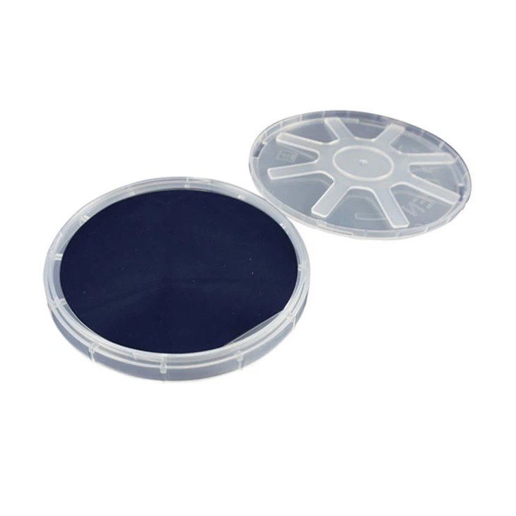
Silicon carbide wafer after above-mentioned cleaning naturally dries on non-dust cloth.Afterwards, 30% hydrogen peroxide solution is heated to approximately 70 ℃, silicon carbide whisker wafer is soaked 3 minutes in hot hydrogen peroxide solution to all the other organic matters that oxidized surface is residual and strong adsorbability material, simultaneously also oxidized generation compact oxidation layer of silicon carbide wafer surface. The wafer taking out is used each 30 seconds of deionized water rinsing positive and negative, removes the hydrogen peroxide solution of remained on surface. The hydrofluoric acid solution of wafer being put into normal temperature soaks 3 minutes, removes surperficial oxide layer. The cleaning step 2 times that repeats above-mentioned oxidation-removal oxidation, makes the pollutant removal on silicon carbide wafer surface clean.
Above-mentioned wafer is taken out rear each 30 seconds of deionized water rinsing positive and negative of using, and removes surperficial residual solution. In dilute sulfuric acid, soak approximately 1 minute, remove surperficial residual metallic and/or metal oxide impurities.
Finally, use each 30 seconds of deionized water rinsing wafer positive and negative, and clean 3-5 minute with ultrasonic oscillation in deionized water, wafer surface is cleaned up completely.
Applications of Silicon Carbide Wafer
Silicon Carbide (SiC) wafers have emerged as a game-changer in the engineering landscape, particularly within power electronics and radio frequency (RF) applications. Their exceptional properties, stemming from the wide bandgap, high breakdown electric field, and superior thermal conductivity, make them ideal for building high-performance, efficient devices.
Revolutionizing Power Electronics
SiC wafers have fundamentally transformed power electronics by enabling the development of advanced devices with unmatched performance:
Higher Voltages, Lower Losses: The wide bandgap of SiC allows operation at higher voltages, reducing energy wasted during switching events and leading to significant efficiency gains.
Compact Designs, Cooler Operation: The high thermal conductivity of SiC efficiently dissipates heat, enabling the creation of compact and lightweight power conversion systems without the need for bulky cooling solutions.
These advantages translate into tangible benefits across various sectors:
Electric Vehicles (EVs): SiC-based traction inverters and on-board chargers contribute to longer driving ranges and faster charging times for EVs by improving power conversion efficiency.
Renewable Energy Systems: SiC devices in solar inverters and wind turbine converters enable more efficient conversion and integration of renewable energy sources into the power grid.
Industrial Motor Drives: SiC-based motor drives offer significant advantages, including higher efficiency, reduced energy consumption, and improved motor reliability in industrial applications.
High-Voltage Direct Current (HVDC) Transmission: SiC devices enable efficient long-distance transmission of electrical power with minimal energy losses.
Mastering the High-Frequency Domain
Beyond power electronics, SiC wafers are making waves in the world of RF and microwave devices:
Unmatched Power Handling: The high electron mobility of SiC allows for superior power handling capability compared to traditional silicon-based devices.
High-Frequency Operation at High Temperatures: The wide bandgap of SiC enables efficient operation at high frequencies and elevated temperatures, crucial for demanding applications.
These characteristics make SiC ideal for:
Power Amplifiers: SiC-based power amplifiers offer higher output power, improved efficiency, and better thermal management compared to silicon counterparts, finding applications in wireless communications, radar systems, and satellite communications.
Radar Systems: SiC technology allows for the development of high-performance radar systems with greater range and resolution due to their ability to handle high power levels and operate at high frequencies, benefiting both military and civilian applications.
Satellite Communications: SiC-based amplifiers and transceivers provide significant advantages in harsh space environments where high power and high-frequency operation are essential for reliable communication.
Wireless Infrastructure: SiC-based devices can unlock higher data rates and improved coverage in wireless infrastructure like base stations and cellular networks while maintaining high efficiency and reliability.
FAQ
We're professional silicon carbide wafer manufacturers and suppliers in China, specialized in providing high quality customized service. We warmly welcome you to wholesale silicon carbide wafer in stock here from our factory. Contact us for quotation.
SiC Dummy Wafer, SiC Epitaxial Wafer, 200mm SiC Wafers