


Product Description
Silicon Carbide (SiC) wafers and substrates are specialized materials used in semiconductor technology made from silicon carbide, a compound known for its high thermal conductivity, excellent mechanical strength, and wide bandgap. Exceptionally hard and lightweight, SiC wafers and substrates provide a robust foundation for fabricating high-power, high-frequency electronic devices, such as power electronics and radio frequency components.
Silicon carbide wafers' unique properties make them ideal for applications requiring high-temperature operation, harsh environments, and improved energy efficiency.
Compared to conventional Si devices, SiC-based power devices have faster switching speeds, higher voltages, lower parasitic resistances, smaller sizes, and less cooling required due to high-temperature capability.

Our silicon carbide wafers are available in a wide range of sizes and specifications, allowing our customers to choose the best option for their specific needs. We offer both bare wafers and epitaxial wafers, and we can customize our products to meet the requirements of any project.
At SiBranch, we are committed to providing our customers with the highest level of service and support. Our team of experts is always available to answer any questions and provide guidance on the best products and solutions for your project. SiBranch offering a wide range of products and services to meet the diverse needs of our clients. Contact us today to learn more about our products and how we can help you achieve your goals.
|
4H N-TYPE SiC 100MM, 350μm WAFER SPECIFICATION |
|||
|
Artic le Number |
W4H100N-4-PO (or CO)-350 |
||
|
Description |
4H SiC Substrate |
||
|
Polytype |
4H |
||
|
Diameter |
(100+0.0-0.5) mm |
||
|
Thickness |
(350±25) μm (Engineering grade ±50μm) |
||
|
Carrier Type |
n-type |
||
|
Dopant |
Nitrogen |
||
|
Resistivity (RT) |
0.012-0.025Ω▪cm (Engineering grade <0.025Ω▪cm) |
||
|
Wafer Orientation |
(4+0.5)° |
||
|
Engineering grade |
Production Grade |
Production Grade |
|
|
2.1 |
2.2 |
2.3 |
|
|
Micropipe Density |
≤30cm-² |
≤10cm-² |
≤1cm-² |
|
Micropipe Free area |
Not specified |
≥96% |
≥96% |
|
Orientation flat (OF) |
|
||
|
Orientation |
Paralle {1-100} ±5° |
||
|
Orientation flat length |
(32.5±2.0) mm |
||
|
ldentification flat (IF) |
|
||
|
Orientation |
Si-face: 90° cw, from orientation flat ±5° |
||
|
ldentification flat length |
(18.0+2.0) mm
|
||
|
Surface |
Option1: Si-face standard polish Epi-ready C-face optical polish |
||
|
Option2: Si-face CMP Epi-ready, C-face optical polish |
|||
|
Package |
Multiple wafer (25) shipping box |
||
|
(Single wafer package upon request) |
|||
|
6H N-TYPE SiC, 2"WAFER SPECIFICATION |
|
|
Artic le Number |
W6H51N-0-PM-250-S |
|
Description |
Production Grade 6H SiC Substrate |
|
Polytype |
6H |
|
Diameter |
(50.8±38) mm |
|
Thickness |
(250±25) um |
|
Carrier Type |
n-type |
|
Dopant |
Nitrogen |
|
Resistivity(RT) |
0.06-0.10Ω▪cm |
|
Wafer Orientation |
(0+0.5)° |
|
Micropipe Density |
≤100cm-² |
|
Orientation flat orientation |
Parallel {1-100} ±5° |
|
Orientation flat length |
(15.88±1.65) mm |
|
Identification flat orientation |
Si-face: 90° cw. frow orientation flat ±5° |
|
ldentification flat length |
(8+1.65) mm |
|
Surface |
Si-face standard polish Epi-ready |
|
C-face matted |
|
|
Package |
Package single wafer package or multiple wafer shipping box |
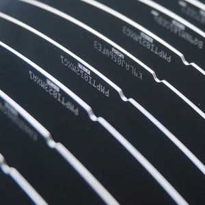
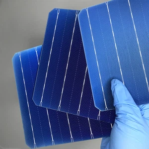
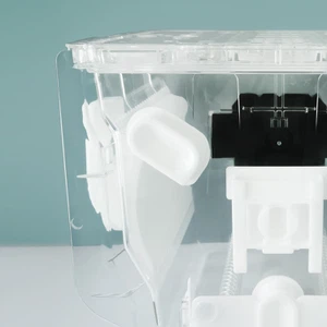
Product Picture


Silicon Carbide (SiC) wafers are a type of semiconductor material used in the production of electronic and optoelectronic devices that require high-temperature, high-voltage, and high-frequency operation. SiC is a wide-bandgap semiconductor material, which means that it has a higher breakdown voltage and can operate at higher temperatures than conventional semiconductors such as silicon.
SiC wafers are typically produced using the physical vapor transport (PVT) or chemical vapor deposition (CVD) methods. In the PVT method, a seed crystal of SiC is placed in a high-temperature furnace and a source material, typically silicon or carbon, is heated until it vaporizes. The vapor is transported by a carrier gas, typically argon, and deposited on the seed crystal, forming a single crystal SiC layer. In the CVD method, a SiC layer is deposited on a substrate by reacting a gas mixture containing silicon and carbon precursors at high temperatures.
Once the SiC crystal is grown, it is sliced into thin wafers and polished to a high degree of flatness and smoothness. The resulting SiC wafers can then be used as a platform for the growth of additional semiconductor layers, which can be doped with impurities to create p-type and n-type regions for device fabrication.
SiC wafers have several advantages over other semiconductor materials such as silicon. SiC has a higher thermal conductivity, which means that it can operate at higher temperatures without suffering from thermal breakdown. Additionally, SiC has a higher breakdown voltage and can operate at higher voltages and frequencies than silicon, making it suitable for applications such as high-power electronics and high-frequency devices.
Deeper Dig into SiC Wafers Properties
The unique electronic band structure of SiC wafers is the key to their exceptional properties. A wide bandgap creates a high hurdle for electrons to overcome, resulting in two key benefits:
High-Temperature Stability: Low intrinsic carrier concentrations mean SiC devices can operate at elevated temperatures without significant leakage currents, ideal for demanding environments.
High Breakdown Electric Field: The wide bandgap also contributes to a strong ability to withstand high voltages, allowing for devices with high blocking voltages and low on-state resistance.
Beyond electrical properties, SiC wafers excel in thermal and mechanical aspects as well.
Efficient Heat Dissipation: The exceptional thermal conductivity allows SiC to efficiently dissipate heat, a critical feature for high-power applications.
Durability in Harsh Environments: High mechanical strength and hardness make SiC resistant to wear and tear, suitable for demanding environments.
SiC comes in various forms called polytypes, distinguished by the stacking arrangement of silicon and carbon atoms. Among these, 4H-SiC and 6H-SiC are most prominent in electronics.
4H-SiC: Preferred for power electronics due to its superior electron mobility and wider bandgap, translating to higher efficiency and performance.
6H-SiC: Finds applications in high-temperature and high-frequency devices due to its higher hole mobility and slightly narrower bandgap.
The choice of polytype hinges on the specific application's needs. Factors like desired electrical properties, operating conditions, and targeted device performance all play a role in selecting the optimal SiC wafer type.
Why Choose Us
Our products are sourced exclusively from the world's top five manufacturers and leading domestic factories. Supported by highly skilled domestic and international technical teams and stringent quality control measures.
Our objective is to provide customers with comprehensive one-on-one support, ensuring smooth channels of communication that are professional, timely, and efficient. We offer a low minimum order quantity and guarantee swift delivery within 24 hours.
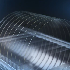
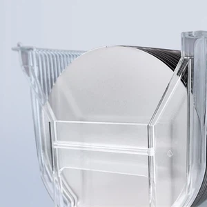
Factory Show
Our vast inventory consists of 1000+ products, ensuring that customers can place orders for as little as one piece. Our self-owned equipments for dicing & backgrinding, and full cooperation in the global industrial chain enable us prompt shipment to ensure customer one-stop satisfaction and convenience.


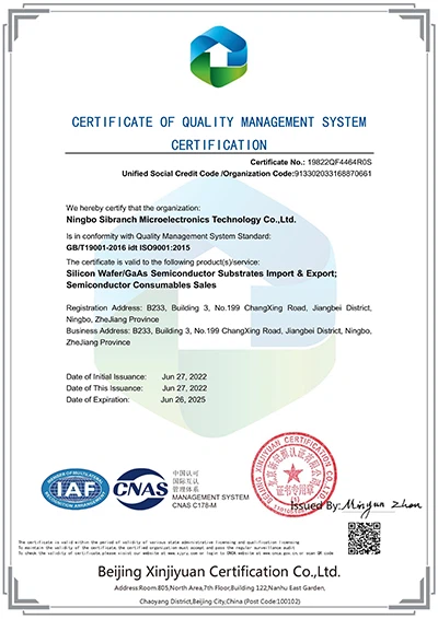
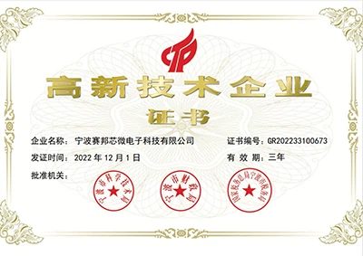
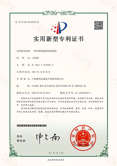
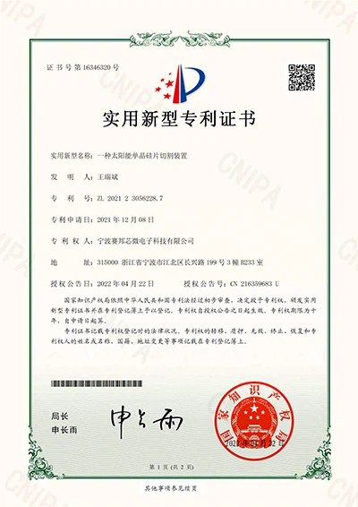
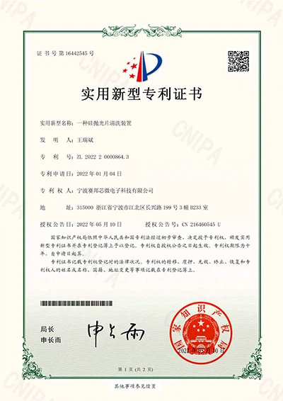
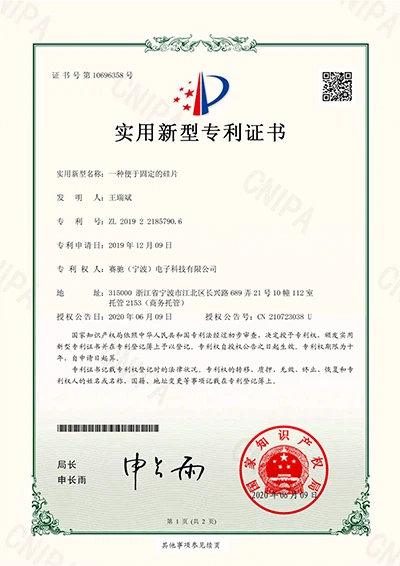
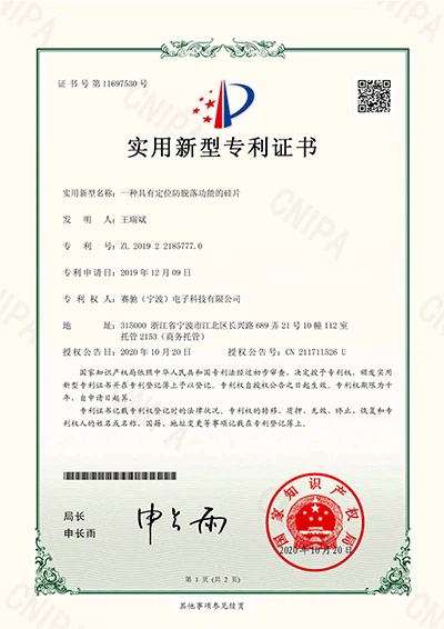
Our Certificate
Our company takes pride in the various certifications we have earned, including our patent certificate, ISO9001 certificate, and National High-Tech Enterprise certificate. These certifications represent our dedication to innovation, quality management, and commitment to excellence.


Hot Tags: sic wafer, China sic wafer manufacturers, suppliers, factory, 200mm SiC Wafers, SiC Epitaxial Wafer, SiC Dummy Wafer, SiC Epitaxial Wafer, 200mm SiC Wafers


