


Ningbo Sibranch Microelectronics Technology Co.,Ltd.:Your Trustworthy 300mm Silicon Wafer Manufacturer!
Founded in 2006 by material science and engineering scientist in Ningbo, China, Sibranch Microelectronics aims to provide semiconductor wafer and service all over the world. Our main products include standard silicon wafers SSP (single side polished), DSP (Double side polished), test silicon wafers and prime silicon wafers, SOI (Silicon on Insulator) wafer and coin roll wafers with diameter up to 12 inch, CZ/MCZ/FZ/NTD, almost any orientation, off cut, high and low resistivity, ultra-flat, ultra-thin, thick wafers etc.
Leading Service
We are committed to constantly innovating our products to provide foreign customers with a large number of high-quality products to exceed customer satisfaction. We can also provide customized services according to customers' requirements such as size, color, appearance, etc. We can provide the most favorable price and high-quality products.
Quality Guaranteed
We have been continuously researching and innovating to meet the needs of different customers. At the same time, we always adhere to strict quality control to ensure that the quality of every product meets international standards.
Wide Sales Countries
We focus on sales in overseas markets. Our products are exported to Europe, America, Southeast Asia, the Middle East and other regions, and are well received by customers around the world.
Various Types of Products
Our company offers customized silicon wafer processing services tailored to meet the specific needs of our clients. These include Si Wafer BackGrinding, Dicing, DownSizing, Edge Grinding, as well as MEMS among others. We strive to deliver bespoke solutions that exceed expectations and ensure customer satisfaction.
Product Types

CZ Silicon Wafers are cut from single crystal silicon ingots pulled using the Czochralski CZ growth method, which is most widely used in the electronics industry to grow silicon crystals from large cylindrical silicon ingots used to manufacture semiconductor devices. In this process, an elongated crystalline silicon seed with precise orientation tolerance is introduced into a silicon molten pool with precisely controlled temperature. The seed crystal is slowly pulled upward from the melt at a strictly controlled rate, and crystal solidification of the liquid phase atoms occurs at the interface. During this pulling process, the seed crystal and the crucible rotate in opposite directions, forming a large single crystal silicon with a perfect crystal structure of the seed.

Silicon oxide wafer is an advanced and essential material used in various high-tech industries and applications. It is a high-purity crystalline substance produced by processing high-quality silicon materials, making it an ideal substrate for many different types of electronic and photonic applications.

Dummy wafers (also called test wafers) are wafers mainly used for experiment and test and are different from general wafers for product. Accordingly, reclaimed wafers are mostly applied as dummy wafers (test wafers).

Gold-coated silicon wafers, and gold-coated silicon chips are used extensively as substrates for analytical characterization of materials. For example, materials deposited onto gold-coated wafers can be analyzed via ellipsometry, Raman spectroscopy or infrared (IR) spectroscopy due to the high-reflectivity and favorable optical properties of gold.

Silicon Epitaxial Wafers are highly versatile and can be manufactured in a range of sizes and thicknesses to suit different industry requirements. They are also used in a variety of applications, including integrated circuits, microprocessors, sensors, power electronics, and photovoltaics.

Manufactured using the latest technology and is designed to offer unparalleled reliability and consistency in performance. Thermal Oxide Dry and Wet is an essential tool for semiconductor manufacturers worldwide as it provides an efficient way to produce high-quality wafers that meet all the demanding requirements of the industry.

This wafer has a diameter of 300 millimeters, making it larger than traditional wafer sizes. This larger size makes it more cost-effective and efficient, allowing for greater production output without sacrificing quality.

The 100mm silicon wafer is a high-quality product that is widely used in the electronics and semiconductor industries. This wafer is designed to provide optimal performance, precision, and reliability that are essential in the manufacturing of semiconductor devices.

The 200mm silicon wafer is also versatile in its applications, with applications in research and development, as well as in high-volume manufacturing. It can be customized to your exact specifications, with options for thin or thick wafers, polished or unpolished surfaces, and other features based on your specific needs.
What is Silicon Wafer Substrate
Silicon wafer substrates are a vital component in manufacturing semiconductor integrated circuits and devices. At their core, they simply provide a solid foundation-literally a substrate-upon which microelectronic circuits can be constructed through intricate photolithography and fabrication steps.
However, silicon substrates impact far more than just giving ICs a flat surface to build on. The crystalline and electronic properties of the substrate wafer itself are crucial in determining the ultimate performance capabilities of devices fabricated on top. Factors such as crystal orientation, chemical purity, lattice defect density, and electrical resistivity characteristics must be tightly controlled and optimized during substrate manufacturing.
Properties of Silicon Wafer Substrate
Resistivity
Resistivity indicates how much the wafer impedes electron flow. Most devices require substrates with precise resistivity ranges. This is achieved by doping the silicon with impurities-most commonly boron (for p-type) or phosphorus (for n-type).
Typical Silicon Wafer Substrate Resistivities:
- 1–30 Ω·cm – low resistivity, used for CMOS logic
- 30–100 Ω·cm – epitaxial substrates
- 1000 Ω·cm – high resistivity, used for RF devices
Flatness/Smoothness
Surface flatness measures how planar the substrate surface is, while smoothness indicates roughness. Both are important for clean photolithography patterning and ensuring devices are built correctly.
- Flatness is quantified using Total Thickness Variation (TTV). Good quality wafers typically have TTV < 10 μm across the wafer.
- Smoothness (roughness) is measured using Root Mean Squared (RMS) roughness. High-end substrates have RMS roughness < 0.5 nm.
Manufacturing of Silicon Wafer Substrate
Producing high-quality silicon wafer substrates is an immense technical challenge requiring advanced manufacturing techniques. Here is a quick overview:
-
Ingot Growth
Everything starts with growing large single-crystal ingots using the Czochralski method. In this process, chunks of ultrapure polysilicon are loaded into a quartz crucible and melted. A tiny single crystal "seed" is lowered until it just touches the molten surface, then slowly withdrawn upwards. As the seed crystal is pulled up, liquid silicon solidifies onto it, allowing a large single crystal to be grown.
Impurity atoms are carefully added to dope the ingot to the specified resistivity. Common dopants are boron and phosphorus. Cooling is precisely controlled to ensure defect-free crystal growth.
-
Slicing
The large single crystal ingot is sliced into individual wafers using internal diameter saws. Diamond-embedded blades continuously cut very thin slices from the entire ingot simultaneously. Cooling fluid is used to minimize damage from friction and heating.
Slicing must be highly precise to ensure uniform wafer thickness and flatness. Target thickness is typically around 0.7 mm for standard diameter wafers.
-
Lapping
After slicing, wafers have moderately rough surfaces. An abrasive lapping process is used to flatten them. This involves forcing each wafer surface against a cast iron lapping plate covered with an abrasive slurry. The plate rotates while precisely controlled pressure is applied to the wafer surface.
Lapping removes material evenly from the surface while flattening any protrusions or ridges left from slicing. This helps improve overall wafer flatness.
-
Etching
Lapping may induce some surface damage up to 10–15 μm deep. This damage is removed by etching the surface using mixtures of acidic or alkaline chemicals. Etching dissolves silicon at a controlled rate to remove lapping damage, leaving a clean, undamaged surface ready for final polishing.
-
Polishing
The final step produces an ultrasmooth, damage-free surface using a chemical mechanical polishing process. This uses similar mechanics to lapping but with alkaline colloidal silica polishing slurry instead of coarse abrasives. The polishing step eliminates subsurface damage from prior processing steps.
Polishing continues until the desired surface RMS roughness specification is reached. Many cycles of precision polishing may be needed to achieve single-digit angstrom roughness.
Common Failure Modes with Silicon Wafer Substrates
Excessive Stress and Cracking
Excessive stress and pressure from scribing, wire bonding, die separation, and packaging operations can cause a silicon wafer to become brittle or crack. This type of failure or damage can affect the durability of the wafer and may render it useless.
Thermal Expansion Mismatch
Thermal expansion refers to the tendency of matter to expand or change its volume, shape, or area due to temperature change. When a substrate is subjected to heat beyond what it can bear, it can result in cracking or breaking, particularly when combined with mismatched materials.
Crystallographic Defects
Existing crystallographic defects-such as dislocations, oxygen precipitates, and stacking faults-in both the silicon wafer and epitaxial layer can compromise wafer quality and lead to device failure. These defects can cause significant abnormal leakage currents or create low-resistance paths that can short-circuit junctions.
Diffusion and Ion Implantation Anomalies
Anomalous diffusion phenomena linked with specific crystal or dopant-defect combinations and contaminant metal precipitate reactions can affect wafer quality and lead to device failure.
Things to Consider When Handling and Storing Silicon Wafer Substrates
Controlled Cleanroom Environment: Maintaining Optimal Conditions
In semiconductor fabrication, cleanroom environments are meticulously controlled to minimize contamination risks and guarantee the highest quality of silicon wafer substrates. These environments typically adhere to strict cleanliness standards, such as ISO Class 1 or Class 10 cleanrooms, where the number of airborne particles is strictly controlled per cubic meter of air.
Cleanrooms have specialized filtration systems that continuously remove particles from the air to maintain optimal conditions. High-efficiency particulate air (HEPA) filters and ultra-low particulate air (ULPA) filters capture particles as small as 0.3 microns and 0.12 microns, respectively.
Mitigating Electrostatic Discharge Risks: Protecting Against Damage
Electrostatic discharge (ESD) poses a significant threat to silicon wafer substrates during handling and storage. Semiconductor facilities implement static control measures such as grounding straps, ionizing air blowers, and conductive flooring to dissipate static charges and prevent damage to wafers.
Personnel wear ground straps to safely discharge static electricity from their bodies, while ionizing air blowers neutralize static charges on wafer surfaces. Conductive flooring materials allow static charges to dissipate harmlessly to the ground, reducing the risk of electrostatic discharge events.
Protective Packaging Solutions: Safeguarding Against Harm
Proper packaging is vital for protecting silicon wafer substrates from physical damage, contamination, and moisture during transit and storage. Semiconductor facilities use various protective packaging solutions to safeguard wafers and maintain their integrity throughout the supply chain.
One common packaging solution is vacuum-sealed packaging, where silicon wafers are placed in a sealed pouch or container and vacuum-sealed to remove air, creating a protective barrier against contaminants and moisture. Desiccant packs are often included in the packaging to absorb residual moisture and maintain a dry environment.
Adherence to Handling Protocols: Precision and Care
Strict adherence to handling protocols is essential to minimize risks during wafer fabrication and assembly. Semiconductor facilities develop detailed handling procedures and protocols that outline best practices for safely transporting, manipulating, and processing silicon wafers.
These handling protocols typically cover a wide range of activities, including wafer loading and unloading, wafer inspection, chemical processing, and mechanical manipulation. They provide step-by-step instructions for each task, specifying the equipment to be used, the proper techniques to be followed, and the safety precautions to be observed.
Tracking and Tracing Systems: Ensuring Accountability and Traceability
Robust identification and tracking systems provide accountability and traceability throughout the semiconductor manufacturing process. These systems assign a unique identifier to each silicon wafer substrate, containing information about its origin, processing history, and quality inspection results.
One common wafer identification method uses barcodes or radio-frequency identification (RFID) tags, applied to wafers at various stages of manufacturing. These identifiers are scanned and recorded at each step of the production process, allowing semiconductor facilities to track the movement and status of wafers in real time.
Optimal Storage Conditions: Preserving Quality Over Time
Proper storage conditions are critical for maintaining the quality and integrity of silicon wafer substrates throughout semiconductor manufacturing. Semiconductor facilities maintain dedicated storage areas within cleanroom environments, equipped with climate-controlled cabinets and racks to preserve wafers under optimal conditions.
Temperature and humidity control are essential for preventing degradation and ensuring the stability of silicon wafers during storage. Semiconductor facilities typically maintain storage temperatures between 18°C and 22°C and humidity levels between 40% and 60% to minimize the risk of moisture-related damage and contamination.
Frequently Asked Questions
Q: How thick is a silicon wafer substrate?
A: Generally, Si wafers have a thickness between 0.4 mm (400 microns) and 0.5 mm. Thinner wafers between 2 and 25 microns in thickness can be required for some specialized scientific and MEMS applications.
Q: What is the difference between a wafer and a substrate?
A: A wafer is a thin, round slice of material, usually made of silicon, that serves as a platform for the fabrication of electronic devices. A substrate is a material that serves as a base for the deposition of another material, such as a thin film or semiconductor device layers. In most semiconductor contexts, "silicon wafer" and "silicon substrate" are used interchangeably, with substrate emphasizing its role as the base material for further processing.
Q: Why is silicon used as a substrate?
A: Silicon is the dominant substrate material for integrated circuits due to its abundant availability, excellent crystalline quality, well-understood manufacturing processes, and beneficial electrical and thermal properties. Its good thermal conductivity helps dissipate heat from operating devices, enhancing overall performance and reliability.
Q: What is the difference between glass substrate and silicon substrate?
A: Glass carrier wafers are used throughout several applications, such as MEMS and semiconductors, particularly for temporary bonding. In comparison to silicon, glass substrate carriers can be made flatter and stiffer, and provide superior thermal stability so that device wafers can be handled safely through processing steps. Glass is also electrically insulating, which can be beneficial for certain applications.
Q: What is the hardness of silicon wafer substrate?
A: Silicon has a Mohs hardness of 7. Its high hardness contributes to its mechanical stability during manufacturing and device operation.
Q: What are the advantages of silicon wafer substrate?
A: Single-crystal silicon is the preferred substrate material for MEMS and semiconductor devices for several reasons: - High mechanical stability - Ease of integrating electronic devices on the same substrate - Young's modulus similar to steel (about 200 GPa) - Low density, making it lighter than many metals (similar to aluminum) - High melting point (1414°C)
Q: How are silicon wafers doped?
A: Doping is the process of introducing controlled amounts of impurity atoms into silicon to modify its electrical resistivity. Common doping methods include: - Diffusion: Wafers are exposed to dopant sources at high temperatures, allowing impurities to diffuse into silicon - Ion implantation: Dopant ions are accelerated and implanted into the silicon substrate with precise control of depth and concentration - In-situ doping: Dopants are added during crystal growth to achieve uniform resistivity throughout the entire ingot
Q: What is the resistivity range of silicon wafer substrate?
A: High-Resistivity Silicon (HRS) substrates are important for low-loss, high-performance microwave and millimeter wave devices in high-frequency telecommunication systems. The highest resistivity-up to ~10,000 Ω·cm-is achieved with Float Zone (FZ) grown silicon, which is produced in smaller quantities and moderate wafer diameters.
Q: What is the difference between silicon and germanium substrate?
A: Germanium exhibits higher temperature sensitivity in its electrical properties compared to silicon. This characteristic can be harnessed for certain sensing applications, but it also means silicon is generally more stable across varying environmental conditions, making it preferred for most commercial semiconductor applications.
Q: What is the thermal conductivity of silicon wafer substrate?
A: The thermal conductivity of silicon is approximately 156 W·m⁻¹·K⁻¹. Thermal conductivity is one of the key properties of semiconductors. It is important to design the thermal properties of an IC in a way that minimizes thermal stress, as silicon chips produce significant amounts of heat during operation.
Q: What is the surface roughness of silicon wafer substrate?
A: The Si wafer surface roughness is achieved through repeated Chemical Mechanical Planarization (CMP) polishing processes. For the polished side of finished wafers, the typical RMS roughness value is <0.5 nm.
Q: What is the function of substrate in semiconductor devices?
A: Substrates are the foundation of electronic devices-materials or structures upon which electronic components are constructed. They provide structural support, facilitate electrical connectivity, and serve as the canvas for the intricate circuitry that powers our modern world.
Q: Is silicon wafer substrate conductive?
A: Silicon is a semiconductor-its electrical conductivity can be controlled through doping, ranging from nearly insulating (high resistivity) to highly conductive (low resistivity). It also has excellent thermal conductivity, which helps dissipate heat in operating devices.
Q: Why is silicon an ideal substrate material?
A: Single-crystal silicon is the preferred substrate material for MEMS and semiconductor devices due to: - High mechanical stability - Ease of integrating electronic devices on the Si substrate - Young's modulus similar to that of steel (about 200 GPa) - Low density, making it as light as aluminum - High melting point, providing excellent thermal stability
Why Choose Us
Our products are sourced exclusively from the world's top five manufacturers and leading domestic factories. Supported by highly skilled domestic and international technical teams and stringent quality control measures.
Our objective is to provide customers with comprehensive one-on-one support, ensuring smooth channels of communication that are professional, timely, and efficient. We offer a low minimum order quantity and guarantee swift delivery within 24 hours.
Factory Show
Our vast inventory consists of 1000+ products, ensuring that customers can place orders for as little as one piece. Our self-owned equipments for dicing & backgrinding, and full cooperation in the global industrial chain enable us prompt shipment to ensure customer one-stop satisfaction and convenience.


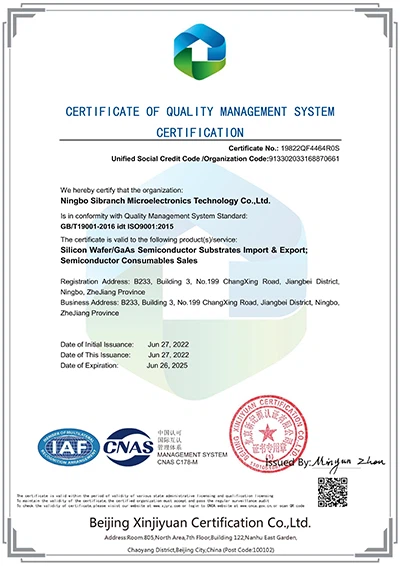
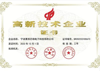
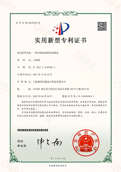
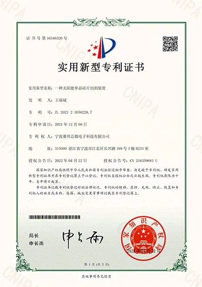
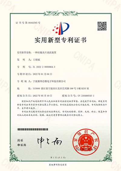
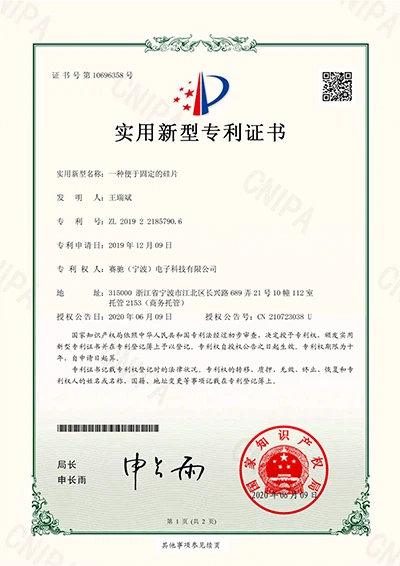
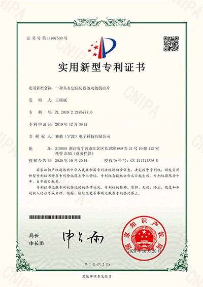
Our Certificate
Our company takes pride in the various certifications we have earned, including our patent certificate, ISO9001 certificate, and National High-Tech Enterprise certificate. These certifications represent our dedication to innovation, quality management, and commitment to excellence.


Hot Tags: silicon wafer substrate, China silicon wafer substrate manufacturers, suppliers, factory, undoped silicon wafer, Gold Coated Silicon Wafer, 12 inch silicon wafers, epitaxial silicon wafer, float zone silicon wafer, thick silicon wafers


