


Product Description

CZ Silicon Wafer
CZ Silicon Wafer are cut from single crystal silicon ingots pulled using the Czochralski CZ growth method, which is most widely used in the electronics industry to grow silicon crystals from large cylindrical silicon ingots used to manufacture semiconductor devices. In this process, an elongated crystalline silicon seed with precise orientation tolerance is introduced into a silicon molten pool with precisely controlled temperature. The seed crystal is slowly pulled upward from the melt at a strictly controlled rate, and crystal solidification of the liquid phase atoms occurs at the interface. During this pulling process, the seed crystal and the crucible rotate in opposite directions, forming a large single crystal silicon with a perfect crystal structure of the seed.
Due to the application of a magnetic field during the standard CZ ingot pulling process, the magnetic field-induced Czochralski MCZ single crystal silicon has relatively low impurity concentrations, low oxygen levels and dislocations, and uniform resistivity changes, and performs well in the manufacture of high-tech electronic components and equipment in the electronics or photovoltaic industries.
one-stop solution
professional team
high quality
|
Growth |
CZ, MCZ, FZ |
|
Grade |
Prime, Test, Dummy, etc. |
|
Diameter |
Other diameters, such as 10mm, 12.7mm, 1.5″, 35mm, 40mm, 2.5″ are also possible |
|
Thickness |
50~3000um |
|
Finish |
As cut, lapped, etched, SSP, DSP, etc |
|
Orientation |
(100) (111) (110) (211) (311) (511) (531) etc. |
|
Off cut |
Up to 4 deg |
|
Type/Dopant |
P/B, N/Phos, N/As, N/Sb, Intrinsic |
|
Resistivity |
FZ: Up to 20k ohm-cm |
|
CZ/MCZ: From 0.001 to 150 ohm-cm |
|
|
Thin films |
* PVD: Al, Cu, Au, Cr, Si, Ni, Fe, Mo, etc. |
|
* PECVD: Oxide, Nitride, SiC, etc. |
|
|
* Silicon epitaxial wafers and epitaxial services (SOS, GaN, GOI etc). |
|
|
Processes |
DSP, ultra thin, ultra flat, etc. |
|
Downsizing, back grinding, dicing, etc. |
|
|
MEMS |
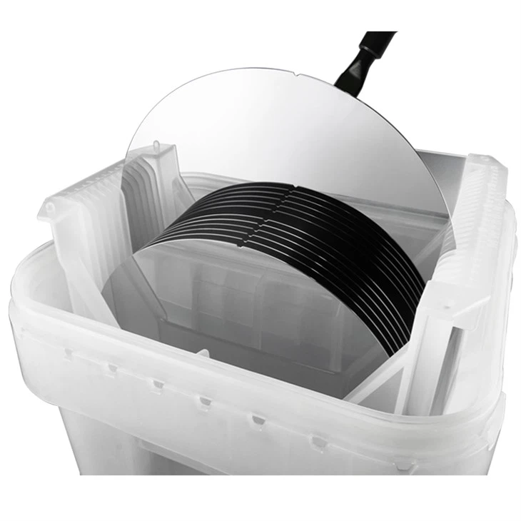
Product Picture

Cz-Si Wafers: History, Properties, Applications
Czochralski silicon (CzSi) wafers are an important type of silicon wafer. Silicon (Si) is a chemical element that makes up about 30% of the Earth's crust. It is the most common naturally occurring element in the world after oxygen and is often used to make microchips and semiconductors. Unlike other elements such as hydrogen, silicon is not a very good conductor of electricity as a whole. However, semiconductors can only be made when silicon is converted into liquid or water.
Silicon wafers are commonly used to form a large number of semiconductor devices. Silicon has been a guiding influence on the electronics and semiconductor industries for decades. Most of them are used for commercial purposes and require little processing. An example of such use is industrial construction using stone, silicon, and clay. Czochralski silicon (CzSi) wafers are also used to produce mortar, stucco concrete (mixed with silica sand). They are used to make ceramics, especially glass. Some of its compounds are used as abrasives.
Properties and Characteristics of Cz-Si Wafers
The properties and characteristics of Czochralski silicon (CzSi) wafers basically cover the standards or requirements that silicon wafers must meet. These properties include electrical, mechanical, chemical, and surface characteristics.
1. Flatness of Cz-Si wafers: Depending on their use, these wafers are usually flat. A flatness of 1-3 microns is acceptable.
2. Size of Cz-Si wafers: Cz-Si wafers are increasing in size, up to 300mm in diameter.
3. Thickness of Cz-Si wafers: The larger the wafer size, the thicker it is, but if the thickness must be increased, the increase in thickness must be less than the increase in diameter.
4. Shape of Cz-Si wafers: Cz-Si wafers are usually round, while their dies are rectangular or square.
5. Orientation grooves: Typically, wafers may contain one or more grooves that provide more information about the wafer. Wafers with a diameter less than 4 inches use two grooves at different locations to show the orientation and semiconductor type of their crystal surface. However, wafers with a diameter of 4 inches have only one groove to show their orientation.
6. Impurity doping: CZ silicon wafers are not completely pure silicon, but are formed by a mixture of atoms doped with impurities (boron, arsenic, antimony or phosphorus) that are added to the concentration and classify the wafers as p-type or n-type
7. Cracks: CZ silicon (CzSi) wafers should be free of damage and various roughness to achieve high performance requirements. Therefore, even if the top layer is rough, the damaged part must be removed.
Why Choose Us
Our products are sourced exclusively from the world's top five manufacturers and leading domestic factories. Supported by highly skilled domestic and international technical teams and stringent quality control measures.
Our objective is to provide customers with comprehensive one-on-one support, ensuring smooth channels of communication that are professional, timely, and efficient. We offer a low minimum order quantity and guarantee swift delivery within 24 hours.
Factory Show
Our vast inventory consists of 1000+ products, ensuring that customers can place orders for as little as one piece. Our self-owned equipments for dicing & backgrinding, and full cooperation in the global industrial chain enable us prompt shipment to ensure customer one-stop satisfaction and convenience.


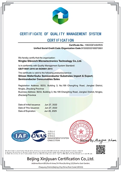
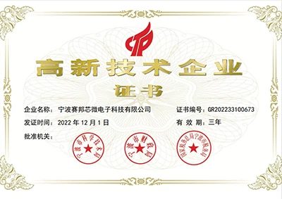
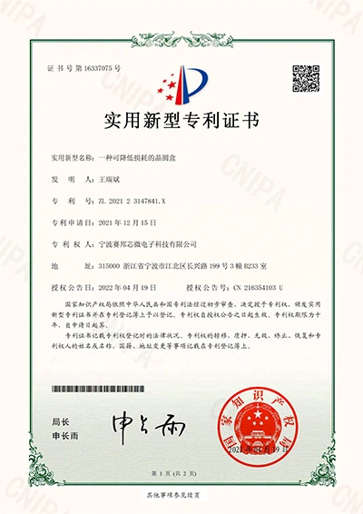
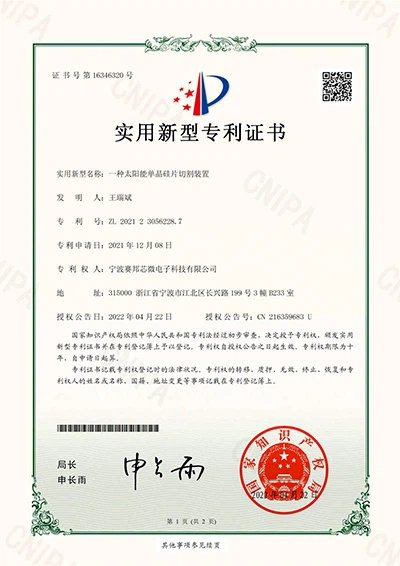
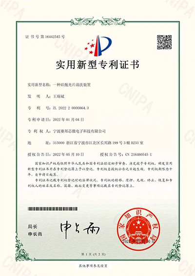
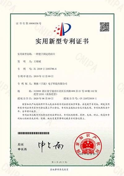
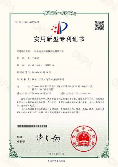
Our Certificate
Our company takes pride in the various certifications we have earned, including our patent certificate, ISO9001 certificate, and National High-Tech Enterprise certificate. These certifications represent our dedication to innovation, quality management, and commitment to excellence.


Hot Tags: cz silicon wafer, China cz silicon wafer manufacturers, suppliers, factory, thick silicon wafers, undoped silicon wafer, 12 inch silicon wafers, float zone silicon wafer, epitaxial silicon wafer, Gold Coated Silicon Wafer


