


Product Description
|
Polished silicon wafer parameters 1 |
||||||
|
Diameter |
1 inch-12 inch |
|||||
|
Thickness |
280um, 300um, 380um, 400um, 500um, 525um, 675um and customize thick |
|||||
|
Type |
P-type and N-type |
|||||
|
Doped |
Undoped, Doped Boron, Doped Phosphorus or Arsenic |
|||||
|
Orientation |
<100>, <111>, <110> |
|||||
|
Resistivity |
1-10ohm.cm, 0.001-0.005ohm.cm, >1000ohm.cm and >20000ohm.cm |
|||||
|
Polish |
DSP |
|||||
|
Method |
CZ and FZ |
|||||
|
Oxide layer |
100, 200, 300nm+/-10% |
|||||
|
Polished silicon wafer parameters 2 |
||||||
|
Diameter |
50.8mm |
76.2mm |
100mm |
125mm |
150mm |
200mm |
|
Diameter tolerance |
±0.4mm |
±0.5mm |
±0.5mm |
±0.3mm |
±0.3mm |
±0.2mm |
|
Thickness |
280um |
381um |
525um |
625um |
675um |
725um |
|
Thick tolerance |
±20um |
±20um |
±20um |
±15um |
±15um |
±15um |
|
TTV |
≦8um |
≦10um |
≦10um |
≦10um |
≦10um |
≦10um |
|
Bending |
≦25um |
≦30um |
≦40um |
≦40um |
≦50um |
≦50um |
|
TIR |
≦5um |
≦6um |
≦6um |
≦5um |
≦5um |
customize |
|
Length of Primary Flat |
16.0±2.0mm |
22.5±2.5mm |
32.5±2.5mm |
42.5±2.5mm |
57.5±2.5mm |
customize |
|
Length of secondary Flat |
8.0±2.0mm |
11.5±1.5mm |
18.0±2.0mm |
27.5±2.5mm |
37.5±2.5mm |
-- |
|
Note: If there are special parameter requirements, can be customized |
||||||
Double side polished silicon wafers are a cutting-edge product that are revolutionizing the semiconductor industry. These wafers go through an intensive polishing process which ensures that they have a smooth, shiny and blemish-free surface on both sides.
The benefits of using double side polished silicon wafers are endless. Firstly, they provide excellent electrical performance which makes them ideal for use in high-performance electronics such as microprocessors and memory devices. Secondly, their high-quality surface allows for more accurate and precise patterning of the semiconductor layers. This, in turn, translates into increased yield and efficiency in the production process.
Furthermore, the double side polishing process gives the wafers greater mechanical strength and durability, meaning that they are able to withstand the rigors of the manufacturing process without any damage. This, in turn, translates into less downtime and fewer losses due to wafer breakage.
In summary, if you want to take your semiconductor manufacturing to the next level, then using double side polished silicon wafers is the way to go. The benefits are numerous, and the quality and reliability of these wafers are unmatched. So why not take advantage of this cutting-edge technology and elevate your production capabilities today?
Product Picture

Why Choose Us
Our products are sourced exclusively from the world's top five manufacturers and leading domestic factories. Supported by highly skilled domestic and international technical teams and stringent quality control measures.
Our objective is to provide customers with comprehensive one-on-one support, ensuring smooth channels of communication that are professional, timely, and efficient. We offer a low minimum order quantity and guarantee swift delivery within 24 hours.
Factory Show
Our vast inventory consists of 1000+ products, ensuring that customers can place orders for as little as one piece. Our self-owned equipments for dicing & backgrinding, and full cooperation in the global industrial chain enable us prompt shipment to ensure customer one-stop satisfaction and convenience.


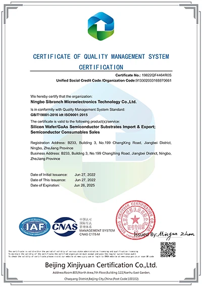
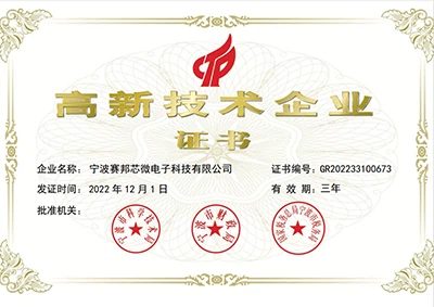
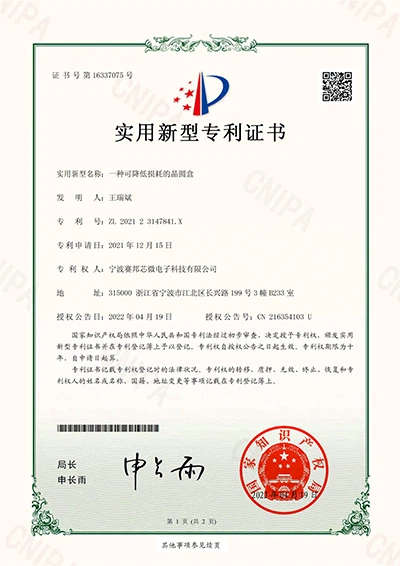
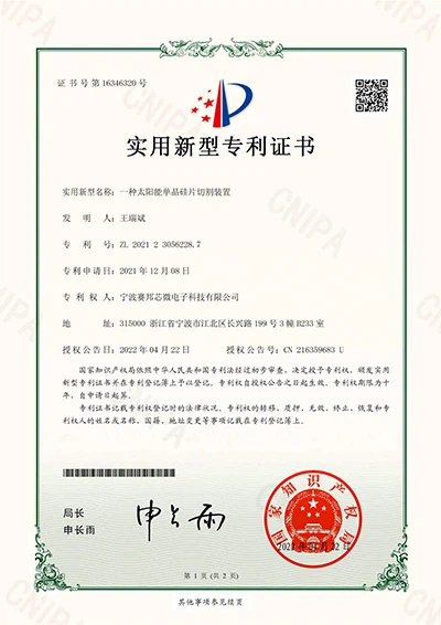
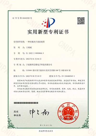
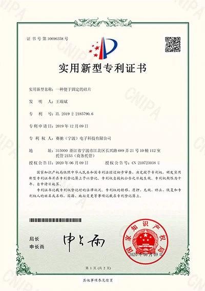
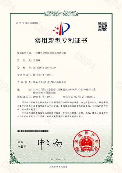
Our Certificate
Our company takes pride in the various certifications we have earned, including our patent certificate, ISO9001 certificate, and National High-Tech Enterprise certificate. These certifications represent our dedication to innovation, quality management, and commitment to excellence.


Hot Tags: double side polished silicon wafers, China double side polished silicon wafers manufacturers, suppliers, factory, 12 inch silicon wafers, Gold Coated Silicon Wafer, float zone silicon wafer, silicon wafer 300mm, 12 Inch Silicon Wafer, undoped silicon wafer


