


Product Description
This wafer has a diameter of 300 millimeters, making it larger than traditional wafer sizes. This larger size makes it more cost-effective and efficient, allowing for greater production output without sacrificing quality.
The 300mm silicon wafer is made from extremely pure silicon, ensuring excellent performance and reliability in a wide range of applications. It offers high precision and uniformity, ensuring consistent performance and quality in every batch.
In terms of mechanical properties, this wafer has excellent flatness and thickness uniformity, resulting in a high yield and low defect rate during production. Its surface is extremely smooth, making it ideal for high-performance applications that require optimum surface quality.
Another advantage of the 300mm silicon wafer is its ability to withstand high temperatures, making it suitable for use in a variety of harsh environments. This feature is particularly beneficial for industries such as aerospace and defense, where components must perform reliably in extreme conditions.
Overall, the 300mm silicon wafer is a top-of-the-line product that offers unparalleled performance and reliability. Its advanced features and benefits make it an essential component in many industries, providing high-quality substrates for a wide range of devices and systems.
|
Growth |
CZ, MCZ, FZ |
|
Grade |
Prime, Test, Dummy, etc. |
|
Diameter |
12 inch / 300mm |
|
Thickness |
600~800um |
|
Finish |
As cut, lapped, DSP (300nm, 200nm, 120nm, 90nm, 65nm, 37nm), etc. |
|
Orientation |
(100) etc. |
|
Off cut |
Up to 4 deg |
|
Type/Dopant |
P/B, N/Phos, N/As, N/Sb, Intrinsic |
|
Resistivity |
CZ/MCZ: From 0.001 to 200 ohm-cm |
|
FZ: Up to 5000 ohm-cm |
|
|
Thin films |
* PVD: Al, Cu, Au, Cr, Si, Ni, Fe, Mo, etc, Coating thicknesses up to 20, 000 Å / ± 5 % |
|
* LPCVD/PECVD: Oxide, Nitride, SiC, etc, Coating thicknesses up to 200, 000 Å / ± 3 % |
|
|
* Silicon epitaxial wafers and epitaxial services (SOS, GaN, GOI etc). |
|
|
Processes |
DSP, ultra thin, ultra flat, etc. |
|
Downsizing, back grinding, dicing, etc. |
|
|
MEMS |
|
Product Picture


Why Choose Us
Our products are sourced exclusively from the world's top five manufacturers and leading domestic factories. Supported by highly skilled domestic and international technical teams and stringent quality control measures.
Our objective is to provide customers with comprehensive one-on-one support, ensuring smooth channels of communication that are professional, timely, and efficient. We offer a low minimum order quantity and guarantee swift delivery within 24 hours.
Factory Show
Our vast inventory consists of 1000+ products, ensuring that customers can place orders for as little as one piece. Our self-owned equipments for dicing & backgrinding, and full cooperation in the global industrial chain enable us prompt shipment to ensure customer one-stop satisfaction and convenience.


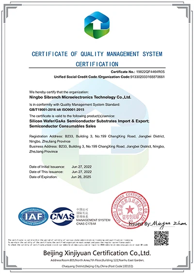
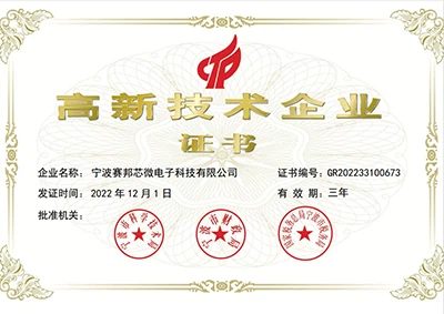
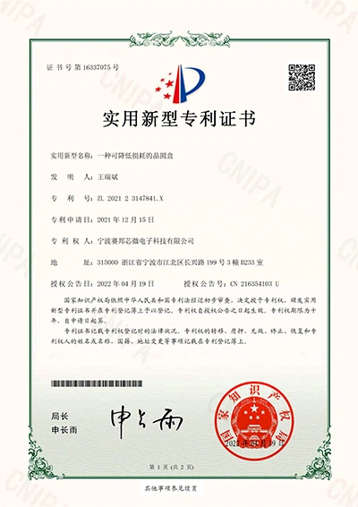
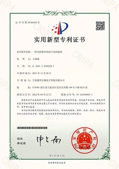
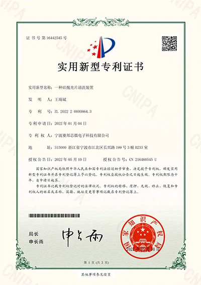
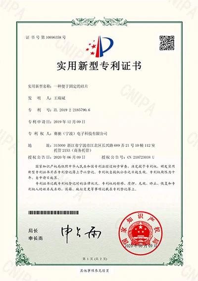
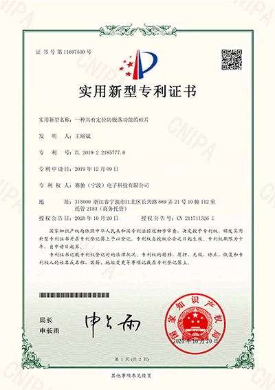
Our Certificate
Our company takes pride in the various certifications we have earned, including our patent certificate, ISO9001 certificate, and National High-Tech Enterprise certificate. These certifications represent our dedication to innovation, quality management, and commitment to excellence.


Hot Tags: 12 inch silicon wafer, China 12 inch silicon wafer manufacturers, suppliers, factory, 12 inch silicon wafers, float zone silicon wafer, silicon wafer 300mm, thick silicon wafers, epitaxial silicon wafer, 450 mm silicon wafer


