





From early planar CMOS processes to advanced FinFETs, p-type substrates continue to be widely used in integrated circuit design. Why does integrated circuit manufacturing prefer p-type silicon?
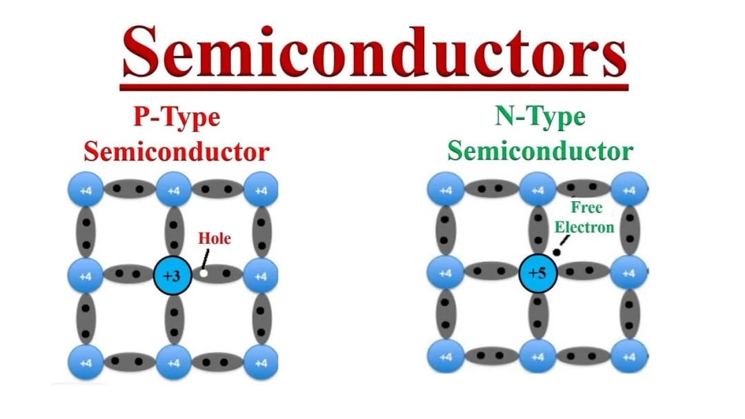
What is P-type silicon and N-type silicon?
Intrinsic silicon has poor electrical conductivity. When pentavalent elements (such as phosphorus P, arsenic As, antimony Sb) are doped into it, an extra "free electron" will be generated. These free electrons can move freely → forming a semiconductor that is mainly electronically conductive, called N-type silicon. When trivalent elements (such as boron B) are doped, since boron atoms have one less valence electron than silicon → "holes" will be formed in the lattice. These holes can move freely and become majority carriers, which are used to build NMOS devices.
What are the historical and practical reasons for using P-type silicon?
1. NMOS devices dominated in the early days
In the 1970s and 1980s, early digital circuits mostly used NMOS-only logic circuits. The NMOS structure is fast and easy to make, and can be directly built on a P-type substrate without the need for an additional well structure; therefore: the P-type substrate is the natural substrate that supports NMOS devices.
2. CMOS technology continues the P-type wafer structure
After the emergence of CMOS technology, NMOS and PMOS must be integrated at the same time: NMOS: still built on a P-type substrate (compatible with the previous NMOS process) PMOS: N-well is built on a P-type substrate to accommodate PMOS This means that only one doping step needs to be added to complete CMOS manufacturing on an existing P-type substrate.
3. Process compatibility and yield control
Using a P-type substrate makes it easier to control latch-up problems; electrons, as minority carriers (in P-type), have a short diffusion distance and are easy to suppress parasitic effects; the substrate grounding design and well isolation structure are also optimized around the P-type silicon process.
4. Fixed substrate potential (simplified bias)
P-type substrate can be directly grounded (GND) as a unified reference potential; if it is an N-type substrate, the substrate must be connected to VDD, which will introduce potential fluctuations due to load changes, causing PMOS VT offset and noise problems.


