






Product Description
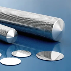
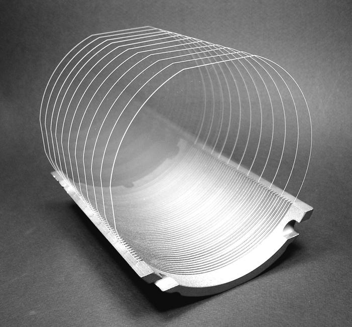
"Fused Silica" or "Fused Quartz" which is the amorphous phase of quartz (SiO2),In contrast to borosilicate glass, fused quartz does not contain any additives; therefore it exists in its pure form, namely SiO2. Fused quartz has a higher transmittance in the infrared and ultraviolet spectra than ordinary glass. Fused quartz is made by melting and resolidifying ultrapure SiO2. Synthetic fused quartz, on the other hand, is made from silicon-rich chemical precursors (such as SiCl4) that are vaporized in an H2 + O2 atmosphere and then oxidized. The SiO2 dust formed in this case fuses to the silicon dioxide on the substrate. Blocks of fused quartz are cut into wafers, which are then finally polished.
Types Of Fused Silica Wafer
Ultraviolet Grade Fused Silica – JGS1
UV grade fused silica wafers have high transparency in the UV spectral range. Transmission for visible and UV light is about 90%, so only losses are due to reflection, and falls to 0% between 220 and 150 nm. In the infrared range, fairly high OH concentrations of typically 1000 ppm result in absorption bands at wavelengths > 1.2 μm.
Optical Grade Fused Quartz – JGS2
The transmission range of the much cheaper JGS2 wafers is shifted towards longer wavelengths compared to the JGS1 wafers. In this case, absorption in the UV starts below wavelengths of about 270 nm, while in the visible and infrared, due to the low OH concentration (typically < 300 ppm), transmission is about 90 % up to a wavelength of about 2 μm.
Full Spectrum Fused Silica – JGS3
These wafers are priced slightly higher than other wafers. They have a very low OH content (typically < 10 ppm) and a high transparency of > 80% in a broad spectral range of about 200 nm – 3 μm and about 90% in the wavelength range of 250 – 2.5 μm.
Main Applications of Fused Silica Wafers
Photomasks
Fused silica wafers are used to make photomasks with high optical clarity for photolithography processes in semiconductor manufacturing
Optics
Precision optical components such as lenses, prisms, filters, aspheric lenses, and diffractive lenses are made from fused silica.
Fiber Optics
Fused silica is the primary material for making optical fibers.
MEMS and Sensors
Fused silica wafers are substrates for making MEMS devices such as accelerometers and optical and biosensors.
Photonics
Specialty fused silica wafers with exacting specifications can be used to make photonic devices such as waveguides and integrated optical circuits.
Semiconductor Carriers/Dummy Wafers
Ultra-smooth fused silica wafers are used as carriers to support device wafers during back grinding and as dummy wafers in process equipment.
High Reliability Electronics
Fused silica provides high insulation and excellent thermal/mechanical stability for aerospace and defense systems.
Medical Devices
Micro-optical and microfluidic systems utilizing fused silica are enabling lab-on-a-chip medical diagnostic devices.
Laser technology
Fused silica's high laser damage threshold is suitable for ultrafast laser systems
|
Material |
Size |
Thickness |
Refractive index |
Material Density |
Expansivity |
Young's modulus Knoop |
Knoop hardness |
|
Unit |
mm |
mm |
nd (20°C) |
g/cm3 |
α (20-300°C) |
kN/mm2 |
HK0.1/20 |
|
BOROFLOAT 33 |
1150 x 850 |
0.7 - 25.4 |
1.4714 |
2.2 |
3.25 x 10⁻⁶ K-1 |
64 |
480 |
|
D 263T Eco |
440 x 360 |
0.1 - 1.1 |
1.5231 |
2.51 |
7.2 x 10⁻⁶ K-1 |
72.9 |
590 |
|
B 270i |
258 x 406 |
0.7 - 17 |
1.523 |
2.56 |
9.4 x10⁻⁶ K-1 |
71.1 |
500 |
|
Wafer |
|
|
Sizes: |
Typically from 1 inch to 4 inch |
|
Thickness: |
Typically 0.5mm and 1.0mm |
|
Clear Aperture: |
Central 90% of diameter |
|
Flatness: |
From 1/4th wave to 2 wave |
|
Parallelism: |
From 5 arcsec to 15 arcsec |
|
Surface Quality: |
10-5 and 20/10 |
|
Rouoghness: |
5 angstrom to 10 angstrom |
|
Material: |
Quartz, LiTaO3, LiNbO3, MgO doped LiNb |
|
Windows |
|
|
Sizes: |
4mm to 300mm |
|
Thickness: |
From 0.3mm to 30mm |
|
Clear Aperture: |
Central 90% of diameter |
|
Flatness: |
1/10th wave |
|
Parallelism: |
1 arcsec |
|
Surface Quality: |
20-10 or better |
|
Shapes: |
Circular, rectangular and special shapes |
|
Material: |
Optical glasses, Fused Silica, B270, D263T, BOROFLOAT 33 |
Product Picture


Why Choose Us
Our products are sourced exclusively from the world's top five manufacturers and leading domestic factories. Supported by highly skilled domestic and international technical teams and stringent quality control measures.
Our objective is to provide customers with comprehensive one-on-one support, ensuring smooth channels of communication that are professional, timely, and efficient. We offer a low minimum order quantity and guarantee swift delivery within 24 hours.
Factory Show
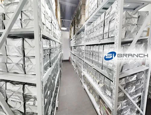
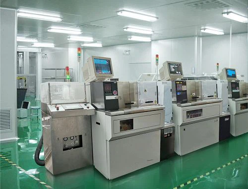
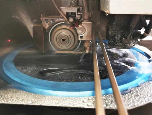
Our vast inventory consists of 1000+ products, ensuring that customers can place orders for as little as one piece. Our self-owned equipments for dicing & backgrinding, and full cooperation in the global industrial chain enable us prompt shipment to ensure customer one-stop satisfaction and convenience.
Our Certificate
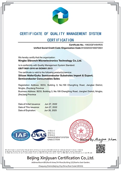
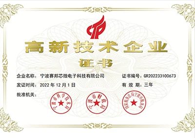
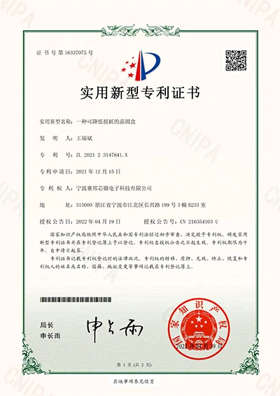
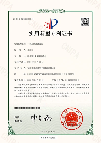
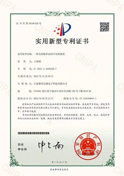
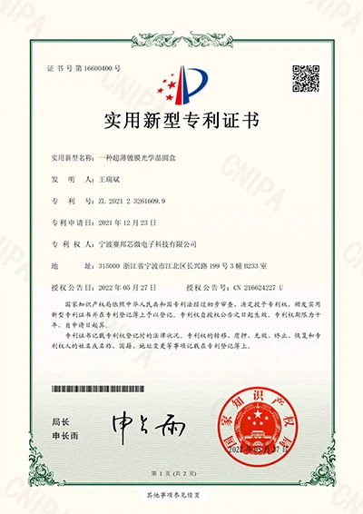
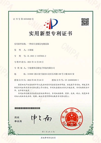
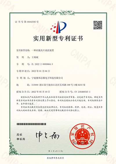
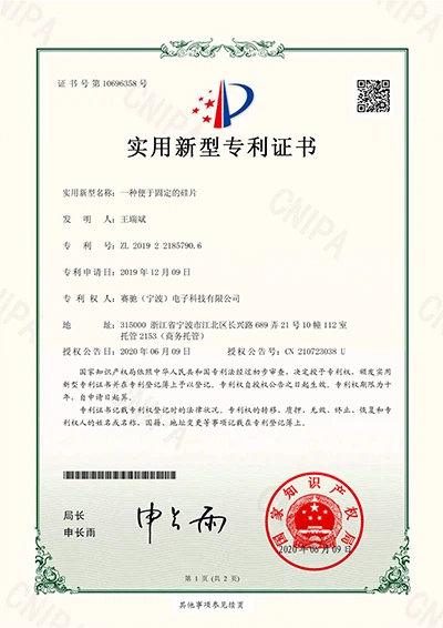
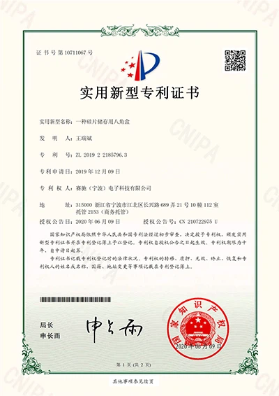
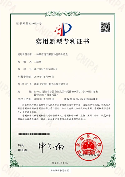
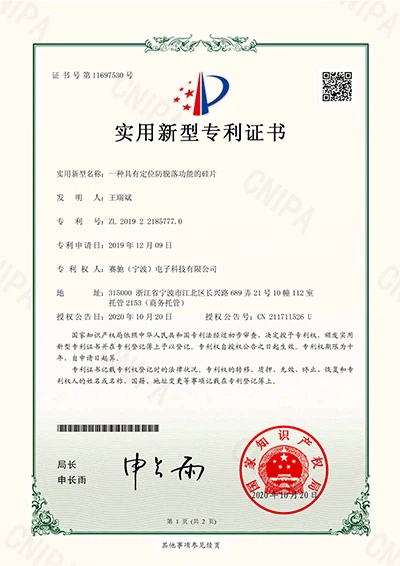
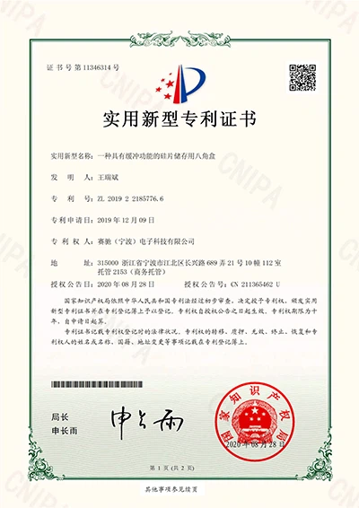
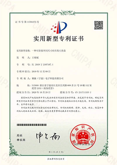
Our company takes pride in the various certifications we have earned, including our patent certificate, ISO9001 certificate, and National High-Tech Enterprise certificate. These certifications represent our dedication to innovation, quality management, and commitment to excellence.
Hot Tags: fused silica wafer, China fused silica wafer manufacturers, suppliers, factory, Fused Silica Wafer


