


Product Description
The use of Silicon-On-Insulator (SOI) wafers in microprocessors is becoming increasingly popular. These types of semiconductors are more efficient, allowing for increased speed and power in microprocessors. SOI wafers are relatively expensive, but they make up for this cost through process savings. The cheapest SOI wafers are typically around 100 mm in diameter, with other diameters available.
We can provide diameter of 2"-12", top silicon thickness of 55nm-500um, buried oxygen layer thickness of 175nm-16um.

Sibranch offers SOI wafers of the following types:
Thick SOI Wafer
This type of wafer has device thickness from 1µm to 300µm.
Ultra-Thin SOI Wafer
This type of wafer has device thickness <500nm.
Ultra-Uniform SOI Wafer
Uniformity of device thickness can be as low as ±0.5µm for thick SOI and ±10nm for ultra-thin SOI.
Ultra-Flat SOI Wafer
This type of SOI has very low BOW/WARP/TTV for specific applications.
|
Diameter |
76, 100mm, 125mm, 150mm, 100mm, 300mm |
|
|
Device Thickness and Max Tolerance |
76mm, 100 mm, 125 mm, and 150 mm |
2-50 +/- .5μm, 0.1~1+/- .025μm |
|
50-150 +/- 1μm |
||
|
>150 +/- 2μm |
||
|
6-50 +/- .5μm |
||
|
200 mm |
50-150 +/- 1μm |
|
|
>150 +/- 2μm |
||
|
Oxide Layer Thickness |
Standard – .5μm, 1μm, and 2μm |
|
Optional – .1 – 10μm |
|
|
Handle Wafer Thickness |
3", 100mm – 300μm and up |
|
125 mm, 150mm – 400μm and up |
|
|
200mm – 500μm and up |
|
|
Tolerance: Standard +/- 25μm |
|
|
Special +/- 5μm |
|
|
Dopants |
N type – Phosphorous, Arsenic, and Antimony |
|
P Type – Boron |
|
|
Resistivities |
Most resistivities available on request including high resistivity Float Zone and low resistivity CZ |
|
Orientation |
<1-0-0> Standard, <1-1-1> and <1-1-0> Optional on request |
|
Standard tolerance +/- .5 degree |
|
|
Special tolerance as low as +/- .1 degree |
|
|
Flat Orientation |
All major flats/Notches are on the <110> Plane +/-.5 degree |
|
Tighter specificatioin available upon request |
|
|
Semi std minor flats are standard on 76.2 and 100mm |
|
|
Finish |
Double side polished standard |
|
Optional backside finishes – nano grind or oxide |
|
|
Coatings |
Oxide and nitride can be supplied on both sides of the wafer. |
|
Optional Ion Implanted Buried Layer |
A buried layer can be implanted in the active layer at the bonding interface. Please check to see if your desired dopant, dopant concentration, and desired energies are available. This service is provided by an outside contractor. |
Product Picture


What are the Applications of Silicon on Insulator?
Silicon on insulator (SOI) can be used in many applications in the electronics sector. These applications include mixed-signal applications, microprocessors, and RF waveguides. Here is a brief introduction on what SOI is and what it is used for. It is a promising material with a variety of applications and is becoming more common.
RF and Mixed-Signal Applications
The global silicon on insulator RF and mixed-signal applications market is segmented by application, region, and technology. North America accounts for the largest share of the industry. Growth in the automotive industry is the major driver. The Middle East and Africa region is expected to register the highest CAGR during the forecast period.
RF and mixed-signal applications of semiconductors are widely seen in cellular technology, consumer electronics, and industrial applications. RF and mixed-signal applications require advanced manufacturing technologies to integrate passive components with digital functions. Embedded non-volatile memory, optical components, and bipolar components can be used in these mixed-signal devices.
Semiconductor on insulator technology reduces junction capacitance and power dissipation, thereby improving performance and reducing power consumption. The resulting silicon on insulator chips operate up to 15% faster than bulk CMOS chips. The technology also increases the speed and power of the device.
Silicon-on-insulator devices can be manufactured using a variety of methods. One of these techniques is to use a seed method, where the topmost layer of silicon is grown directly on the insulator. Silicon-on-insulator devices are produced using diamond-tipped tools.
High purity and uniformity of semiconductors are essential for RF devices. The thickness of the substrate is also critical for frequency response. Therefore, both the substrate and the RF components must be optimized. However, the specifications of RF devices and substrates vary greatly over time, so this variation must be considered when designing the device. One way to minimize variation is to use engineered substrates.
RF Waveguides
The global silicon-on-insulator market is segmented into three segments: technology, application, and region. In terms of region, North America is the largest region, accounting for about 80% of the total market. Meanwhile, Europe is segmented into three sub-regions: Italy, France, and the rest of Europe. Furthermore, the Asia-Pacific region is further segmented into South Asia and Latin America. The Middle East and Africa region is similarly segmented into two segments: type and size.
The manufacturing process of silicon-on-insulator is relatively simple and inexpensive, requiring minimal labor and materials. It also allows for precise control of the silicon layer thickness, which improves device performance and protects it from environmental factors. These are just a few of the many advantages of silicon-on-insulator manufacturing.
Silicon-on-insulator waveguides are a promising technology for RF and optical applications. The technology offers several advantages over conventional silicon waveguides, including the ability to integrate multiple functions on a single chip. For example, silicon waveguides can be used to build ultra-high frequency antennas.
The silicon-on-insulator market is segmented by technology, application, product, and region. Automotive and consumer electronics are the major application areas for silicon-on-insulator. The automotive and consumer electronics sectors are experiencing rapid growth. The technology for manufacturing silicon-on-insulator is very flexible and can be customized to the specific needs of different industries.
RF Amplifiers
The silicon-on-insulator market is segmented by technology, region, and application. In 2018, the North American market held the largest share, followed by the European market (including the UK, France, and Italy) and the Asia-Pacific market (including Latin America and the GCC). In addition, the Middle East and Africa markets are expected to witness significant growth over the next five years.
The number of transistors used in a silicon-on-insulator (SOI) power amplifier is limited by the breakdown voltage, which is typically between 80 and 300V. The breakdown voltage reduces the signal current of each transistor, thus improving amplifier efficiency. However, this approach only works when both silicon layers have the same phase.
Another advantage of SOI technology is the ability to integrate components into a single chip. The SOI layer eliminates the need for metal interconnects. This helps reduce the cycle time for manufacturing products. SOI technology also enables significantly reduced RF losses.
Another benefit of SOI technology is the ability to manufacture high-frequency devices. RF amplifiers using SOI devices require broadband power, and SOI technology is well suited for this purpose. To achieve this, dynamically biased silicon transistors are used in a stack of different topologies. This reduces gate oxide breakdown and improves output power. In addition, the power performance of SOI devices is enhanced by the inclusion of a series transformer.
RF Transceivers
SOI is an excellent choice for RF transceivers due to its excellent performance characteristics. It provides excellent insertion loss and linearity while offering CMOS efficiency and low power consumption. In addition, it enables faster data transmission for applications such as car-to-car communications and virtual reality. In addition, it is cost-effective and allows multiple power amplifiers to be stacked in a single chip.
The process of silicon-on-insulator devices is based on a two-layer process. The first layer is oxidized while the second layer is deposited on top. This step-by-step process is called smart cut and involves controlled lift-off and ion implantation.
The second layer consists of transistors and capacitors. They are connected in series. This enables the device to have an integrated transmitter and receiver. In addition, it has body biasing capabilities, which enables it to provide excellent performance and energy efficiency. It also provides excellent reliability in automotive applications.
SOI has high resistivity properties that help reduce substrate losses. Its resistivity can be as high as 1 kO*cm. This makes SOI an ideal substrate for RF integrated circuits and mixed-signal applications. In addition, its low power consumption and broadband capabilities make it a valuable choice for mobile electronics and other RF transceivers.
CMOS technology is another choice for RF transceivers. It allows the use of multiple active devices and has a high Q value. In addition, the process supports high-value polysilicon resistors, high-current inductors, and MOM capacitors.
Radio Frequency (RF) Filters
RF filters using Silicon-On-Insulator (SOI) technology offer several advantages over conventional RF filters. This technology enables small size, high power handling, and a wide tuning range. It also has the advantage of avoiding the nonlinearity of varactor filters and the size limitations of switched filter banks. This type of RF filter can also be programmed via a three-wire serial control interface. Its features include five-bit tuning resolution, center frequency and bandwidth tuning, and reflection coefficient tuning. In addition to these advantages, this type of RF filter consumes less than 50 mW of power.
RF filters using SOI substrates can also be mounted using flip-chip components. The flip-chip mounting method helps minimize signal loss between the SOI substrate and the filter. This mounting method also enables higher performance and reduces parasitic effects. In addition, SOI substrates are inexpensive and suitable for use in highly sensitive devices.
A thin silicon layer is used as the core of the filter. The SOI layer has a high refractive index and a small size. It also enables multiple functions to be implemented on a single chip. However, silicon waveguides are sensitive to fabrication defects and sidewall roughness, which increase losses and induce phase errors.
Why Choose Us
Our products are sourced exclusively from the world's top five manufacturers and leading domestic factories. Supported by highly skilled domestic and international technical teams and stringent quality control measures.
Our objective is to provide customers with comprehensive one-on-one support, ensuring smooth channels of communication that are professional, timely, and efficient. We offer a low minimum order quantity and guarantee swift delivery within 24 hours.
Factory Show
Our vast inventory consists of 1000+ products, ensuring that customers can place orders for as little as one piece. Our self-owned equipments for dicing & backgrinding, and full cooperation in the global industrial chain enable us prompt shipment to ensure customer one-stop satisfaction and convenience.


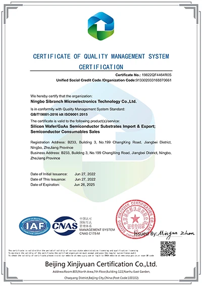
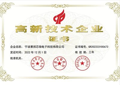
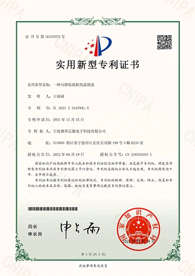
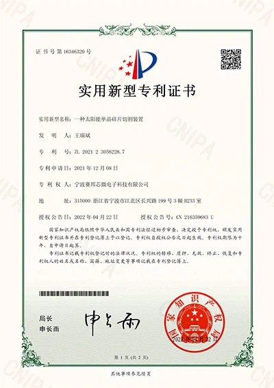
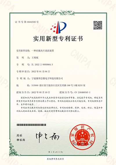
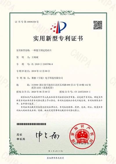
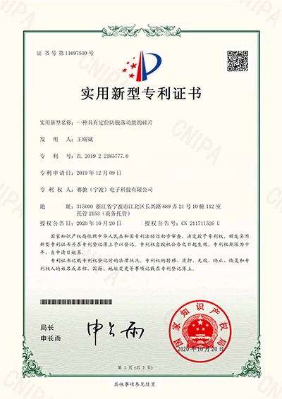
Our Certificate
Our company takes pride in the various certifications we have earned, including our patent certificate, ISO9001 certificate, and National High-Tech Enterprise certificate. These certifications represent our dedication to innovation, quality management, and commitment to excellence.


Hot Tags: silicon on insulator wafer, China silicon on insulator wafer manufacturers, suppliers, factory, SOI Silicon On Insulator, , , SOI Silicon On Insulator


