


Technical Parameters of Protos Spacer (for Wafer use)
Spacer For Wafer Use is also called anti-static stacking pad, silicon wafer paper, semiconductor wafer box inner pad, solar wafer buffer pad, semiconductor wafer box inner pad, PCB buffer pad, conductive pad, black wafer pad, anti-static wafer pad, conductive wafer pad, round wafer pad, wafer block, and its surface treatment process is also called anti-static black embossed wafer pad, embossed wafer block, etc.
This product is made of permanent conductive or anti-static film by hot pressing and die cutting. The surface of the film can be made smooth or made into various patterns according to requirements. The product can be made into any size and shape according to requirements, and the finished product has good dimensional stability, neat appearance, no powder loss, and no dust. The raised pattern wafer gasket can not only effectively prevent the product from being damaged by static electricity, but also play a certain buffering role.

|
Item |
ASTM American Society for Testing Materials ASTM |
GB Test standard |
Unit |
Test result |
|
Melt index |
D1238 |
GB3682 |
g/10min |
2.1 |
|
Water absorption |
D570 |
GB/96-04-10 |
% |
0.5 |
|
Density |
/ |
GB1033 |
g/cm |
0.98 |
|
Tensile strength |
TD MD |
GB/96-04-10 |
MPa |
TD: 32.01 MD: 33.75 |
|
Breaking elongation rate |
TD MD |
GB/96-04-10 |
% |
TD: 702 MD: 685 |
|
Surface resistivity |
/ |
GJB2605-1996 <1×10¹²Ω/square |
Ω/square |
105-9 |
|
Friction coefficient |
Outer surface |
GB/96-04-10 |
Us |
0.09 |
|
Inner surface |
Ud |
0.08 |
||
|
Static dissipation |
5000-0V |
SJ/T10694-1996 |
Sec. |
<2 |
|
Heat seal temperature |
/ |
GB/96-04-10 |
F |
250-375 |
|
Capacitance release |
E1A541 |
SJ/T10694-1996 |
V |
<15KV Voltage difference-E1A541 |
|
Size |
GB/96-04-10 |
Thickness 0.1±0.01mm Diameter (100~300)±2mm |
||
|
Appearance |
GB/96-04-10 |
No layering, wrinkles, warping, cracking, adhesion, foreign body attached |
||
The primary benefits of using spacers is that it helps to control the gap between the wafers with an accuracy of a few micrometers. This tiny gap is essential for the proper functioning of the semiconductor device. Spacers also help to prevent contact between the wafers, which could lead to damage or contamination.
Product Picture


Why Choose Us
Our products are sourced exclusively from the world's top five manufacturers and leading domestic factories. Supported by highly skilled domestic and international technical teams and stringent quality control measures.
Our objective is to provide customers with comprehensive one-on-one support, ensuring smooth channels of communication that are professional, timely, and efficient. We offer a low minimum order quantity and guarantee swift delivery within 24 hours.
Factory Show
Our vast inventory consists of 1000+ products, ensuring that customers can place orders for as little as one piece. Our self-owned equipments for dicing & backgrinding, and full cooperation in the global industrial chain enable us prompt shipment to ensure customer one-stop satisfaction and convenience.


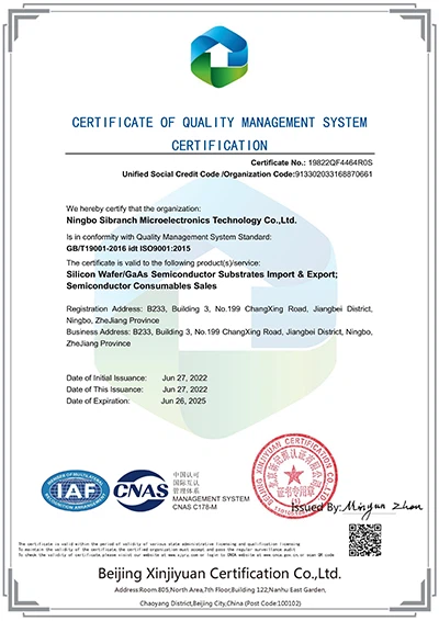
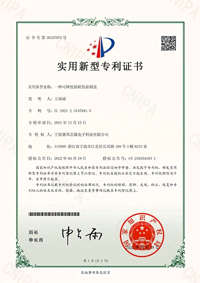
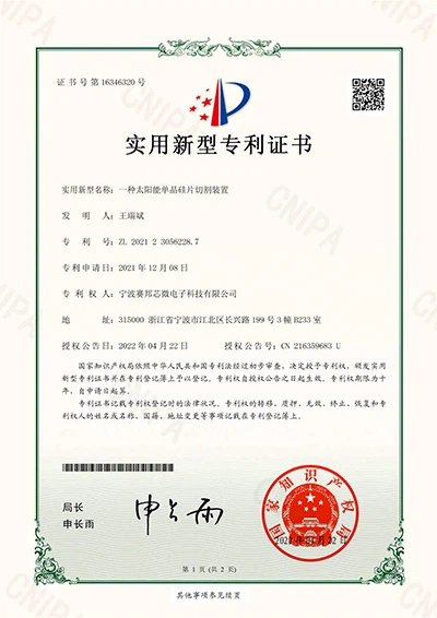
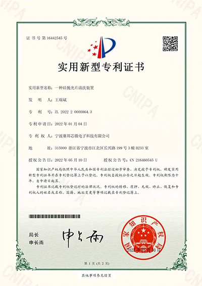
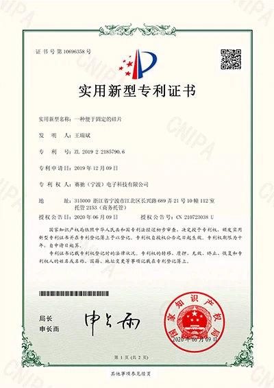
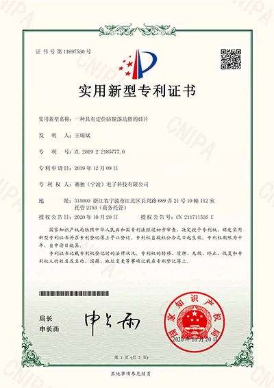
Our Certificate
Our company takes pride in the various certifications we have earned, including our patent certificate, ISO9001 certificate, and National High-Tech Enterprise certificate. These certifications represent our dedication to innovation, quality management, and commitment to excellence.


Hot Tags: spacer for wafer use, China spacer for wafer use manufacturers, suppliers, factory, Horizontal Wafer Shipper Wafer Stack Box


