


Product Description
SOI stands for silicon-on-insulator, An SOI wafer is made up of 3 basic layers, a device layer, a BOX layer and a Handle layer. The BOX layer also called the Buried Oxide layer is trapped between the Device layer and the Handle layer.
Transistors form within the top, device layer which are the center of SOI wafer's speed and efficiency. These transistors are not only great when it comes to conserving power but are shielded from external factors like cosmic rays and radioactive interferences, leading to reduced data loss.
SOI silicon wafers are ideal for high-performance ICs, such as microprocessors, because they provide a more stable and reliable foundation for the circuitry. Additionally, they are well-suited for wireless communication devices, which require low power consumption and high speed data transfer in order to function efficiently.
Overall, SOI silicon wafers offer significant advantages over traditional silicon wafers, making them a critical component in the manufacture of modern electronics.
We can provide diameter of 2"-12", top silicon thickness of 55nm-500um, buried oxygen layer thickness of 175nm-16um.
Sibranch offers SOI wafers of the following types:
Thick SOI Wafer
This type of wafer has device thickness from 1µm to 300µm.
Ultra-Thin SOI Wafer
This type of wafer has device thickness <500nm.
Ultra-Uniform SOI Wafer
Uniformity of device thickness can be as low as ±0.5µm for thick SOI and ±10nm for ultra-thin SOI.
Ultra-Flat SOI Wafer
This type of SOI has very low BOW/WARP/TTV for specific applications.
|
Diameter |
76, 100mm, 125mm, 150mm, 100mm, 300mm |
|
|
Device Thickness and Max Tolerance |
76mm, 100 mm, 125 mm, and 150 mm |
2-50 +/- .5μm, 0.1~1+/- .025μm |
|
50-150 +/- 1μm |
||
|
>150 +/- 2μm |
||
|
6-50 +/- .5μm |
||
|
200 mm |
50-150 +/- 1μm |
|
|
>150 +/- 2μm |
||
|
Oxide Layer Thickness |
Standard – .5μm, 1μm, and 2μm |
|
Optional – .1 – 10μm |
|
|
Handle Wafer Thickness |
3", 100mm – 300μm and up |
|
125 mm, 150mm – 400μm and up |
|
|
200mm – 500μm and up |
|
|
Tolerance: Standard +/- 25μm |
|
|
Special +/- 5μm |
|
|
Dopants |
N type – Phosphorous, Arsenic, and Antimony |
|
P Type – Boron |
|
|
Resistivities |
Most resistivities available on request including high resistivity Float Zone and low resistivity CZ |
|
Orientation |
<1-0-0> Standard, <1-1-1> and <1-1-0> Optional on request |
|
Standard tolerance +/- .5 degree |
|
|
Special tolerance as low as +/- .1 degree |
|
|
Flat Orientation |
All major flats/Notches are on the <110> Plane +/-.5 degree |
|
Tighter specificatioin available upon request |
|
|
Semi std minor flats are standard on 76.2 and 100mm |
|
|
Finish |
Double side polished standard |
|
Optional backside finishes – nano grind or oxide |
|
|
Coatings |
Oxide and nitride can be supplied on both sides of the wafer. |
|
Optional Ion Implanted Buried Layer |
A buried layer can be implanted in the active layer at the bonding interface. Please check to see if your desired dopant, dopant concentration, and desired energies are available. This service is provided by an outside contractor. |
Product Picture


Why Choose Us
Our products are sourced exclusively from the world's top five manufacturers and leading domestic factories. Supported by highly skilled domestic and international technical teams and stringent quality control measures.
Our objective is to provide customers with comprehensive one-on-one support, ensuring smooth channels of communication that are professional, timely, and efficient. We offer a low minimum order quantity and guarantee swift delivery within 24 hours.
Factory Show
Our vast inventory consists of 1000+ products, ensuring that customers can place orders for as little as one piece. Our self-owned equipments for dicing & backgrinding, and full cooperation in the global industrial chain enable us prompt shipment to ensure customer one-stop satisfaction and convenience.


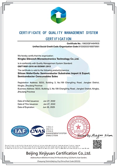
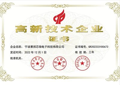
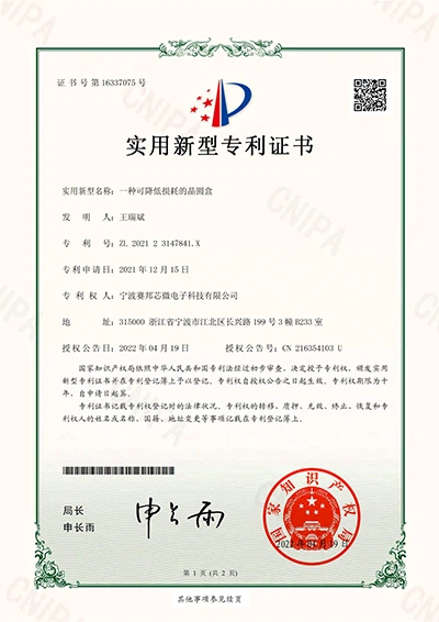
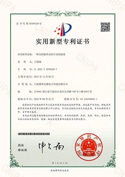
Our Certificate
Our company takes pride in the various certifications we have earned, including our patent certificate, ISO9001 certificate, and National High-Tech Enterprise certificate. These certifications represent our dedication to innovation, quality management, and commitment to excellence.


Hot Tags: soi silicon on insulator, China soi silicon on insulator manufacturers, suppliers, factory, SOI Silicon On Insulator, SOI Silicon On Insulator, SOI Silicon On Insulator


