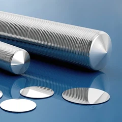
Silicon wafers are one of the most important raw materials in the electronics industry, mainly used to manufacture integrated circuits, capacitors, diodes and other components. Integrated circuits are tiny circuits composed of a large number of basic components such as transistors, capacitors, resistors, etc., which can be used in various electronic devices such as computers, communication equipment, and entertainment equipment. Semiconductor silicon wafers are one of the core materials for manufacturing integrated circuits. The size of semiconductor silicon wafers is divided into 2 inches (50.8mm), 4 inches (100mm), 6 inches (150mm), 8 inches (200mm), and 12 inches (300mm) according to the diameter. Different silicon wafer sizes and processes are used for different semiconductor products.

Advantages of large-size silicon wafers
The number of chips manufactured on a single silicon wafer increases: The larger the wafer, the less waste there is at the edges, which improves the utilization rate of the silicon wafer and reduces costs. Taking 300mm silicon wafers as an example, its available area is twice that of 200mm silicon wafers under the same process, which can provide a productivity advantage of up to 2.5 times the number of chips.
The overall utilization rate of silicon wafers is improved: Making rectangular silicon wafers on round silicon wafers will make some areas at the edges of the silicon wafers unusable, and the increase in the size of the silicon wafers reduces the loss ratio of unused edges.
Equipment capacity is improved: Under the condition that the basic process flow: thin film deposition → lithography → etching → cleaning and other basic development conditions remain unchanged, the average production time of a chip is shortened, the equipment utilization rate is improved, and the company's production capacity is expanded.


