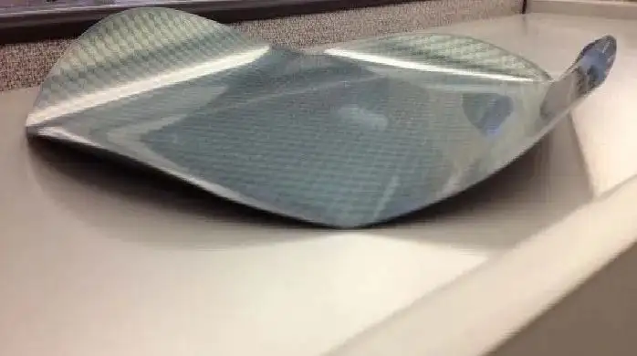
Yesterday, a student in Knowledge Planet asked what the silicon wafer surface parameters Bow, Warp, TTV, etc. are and how to distinguish them. I think this question is quite representative, so I wrote a special article to explain it.

Wafer surface parameters Bow, Warp, and TTV are very important factors that must be considered in chip manufacturing. These three parameters together reflect the flatness and thickness uniformity of the silicon wafer and have a direct impact on many key steps in the chip manufacturing process.
What are TTV, Bow, Warp?
TTV(Total Thickness Variation)

TTV is the difference between the maximum and minimum thickness of a silicon wafer. This parameter is an important indicator used to measure the uniformity of silicon wafer thickness. In semiconductor manufacturing, the thickness of a silicon wafer must be very uniform across the entire surface. It is usually measured at five locations on the silicon wafer and the maximum difference is calculated. Ultimately, this value is the basis for judging the quality of the silicon wafer. In practical applications, the TTV of a 4-inch silicon wafer is generally less than 2um, and that of a 6-inch silicon wafer is generally less than 3um.

Bow
Bow refers to the curvature of a silicon wafer in semiconductor manufacturing. The word may come from the description of the shape of an object when it is bent, just like the curved shape of a bow. The value of Bow is defined by measuring the maximum deviation between the center and edge of the silicon wafer. This value is usually expressed in microns (µm). The SEMI standard for 4-inch silicon wafers is Bow<40um.

Warp
Warp is a global characteristic of silicon wafers, indicating the maximum deviation of the silicon wafer surface from the plane. It measures the distance between the silicon wafer's highest and lowest point of the silicon wafer. The SEMI standard for 4-inch silicon wafers is Warp < 40um.

What are the differences between TTV, Bow, and Warp?
TTV focuses on the change in thickness and does not care about the bow or twist of the wafer.
Bow focuses on the overall bow, mainly considering the bow between the center point and the edge.
Warp is more comprehensive, including the bow and twist of the entire wafer surface.
Although these three parameters are all related to the shape and geometric characteristics of the silicon wafer, they measure and describe different aspects and have different effects on semiconductor processes and wafer handling.

Impact of TTV, Bow, and Warp on semiconductor process
First of all, the smaller the three parameters, the better. The larger the TTV, Bow, and Warp, the greater the negative impact on the semiconductor process. Therefore, if the values of the three exceed the standard, the silicon wafer will be scrapped.
Impact on the photolithography process:
Depth of focus problem: During the photolithography process, it may cause changes in the depth of focus, affecting the pattern's clarity.
Alignment problem: It may cause the wafer to shift during the alignment process, further affecting the alignment accuracy between layers.

Impact on chemical mechanical polishing:
Uneven polishing: It may cause uneven polishing during the CMP process, resulting in surface roughness and residual stress.
Impact on thin film deposition:
Uneven deposition: Concave and convex wafers may cause uneven thickness of deposited films during deposition.
Impact on wafer loading:
Loading problems: Concave and convex wafers may cause wafer damage during automatic loading


