Dummy Wafers
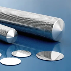
The word "dummy" means "fake" or "simulated." Dummy wafers, also known as fake wafers, typically have no pattern or only a few patterned layers. Their main application scenarios are:
Used for debugging and calibrating semiconductor equipment to ensure it is in optimal condition before formal production.
Used when introducing new processes or adjusting existing ones, allowing for testing and optimization to reduce risks to mass production wafers.
Test Wafers
Test wafers (also called engineering wafers) go through the full process flow and contain various patterns and structures. Their main functions are:
During the introduction of new chip products, test wafers are used to verify and optimize the manufacturing process, ultimately enabling mass production.
When process issues occur with mass production wafers, test wafers are used for corresponding DOE (Design of Experiments) testing to help improve the process.
Mass Production Wafers
Mass production wafers are used to produce semiconductor devices that are shipped to customers. These wafers undergo strict quality control during the production process to ensure that the final products meet customer requirements.
Why are these types of wafers categorized separately?
The distinction is mainly based on cost and importance. In terms of cost and criticality:
Mass production wafers > Test wafers > Dummy wafers.
Mass production wafers are shipped to customers and represent the economic lifeline of the entire company. It is essential that they complete production with both high quality and high yield. Their process parameters and workflows are relatively fixed, and any changes must be 100% safe and reliable.
Therefore, lower-cost and more flexible dummy wafers and engineering (ENG) wafers are used to avoid wasting valuable mass production wafers during testing and process optimization.


