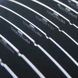
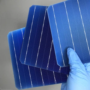
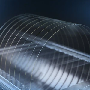
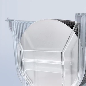
Wafers made of silicon on insulator (SOI) are produced using three primary methods: epitaxial layer transfer, bonded SOI, and silicon on insulator. Every technique has certain advantages and benefits of its own.
First off, a layer of silicon can be created on top of an insulating layer, such silicon dioxide, using the silicon on insulator technique. With this method, the top silicon layer and the underlying substrate are separated by a buried oxide layer that is created via ion implantation. This method works especially well for producing wafers with outstanding thermal conductivity and homogeneous layers.
Second, a thin layer of premium silicon is bonded onto an insulator substrate using the bonded SOI process. This is accomplished by attaching a thin layer of silicon onto a substrate after it has been created via ion implantation or epitaxial growth. This process makes it possible to create highly integrated circuits and is perfect for producing wafers with specific thicknesses.
Lastly, another method for producing SOI wafers is epitaxial layer transfer. Using epitaxial growth techniques, a thin layer of silicon is formed on a donor substrate in this process. Subsequently, this layer is bonded onto an insulating substrate via chemical mechanical polishing and wafer bonding. A superior SOI wafer with exceptional electrical characteristics is the end product.

