


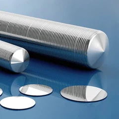




Introduction: The Unsung Hero of the Digital Age
Every smartphone, computer, and cloud server begins its life not as a complex circuit, but as an exquisitely engineered slice of crystalline silicon: the wafer. While transistors and architectures capture headlines, the quality of the underlying silicon wafer is the absolute determinant of final chip performance, power efficiency, and manufacturing yield. For fab managers and technical purchasers, selecting the right wafer is the first and most critical decision in the semiconductor supply chain. This guide demystifies the science behind silicon wafer manufacturing, providing a framework to specify the optimal substrate for your application.
Chapter 1: The Birth of Crystal: Growth Methods Compared
The journey starts with hyper-pure electronic-grade polysilicon, melted and transformed into a single, flawless crystal.
- The Czochralski (CZ) Method: The workhorse of the industry, accounting for over 90% of all silicon wafers. A seed crystal is dipped into molten silicon and slowly pulled, rotating to form a large-diameter ingot. Magnetic Czochralski (MCZ) applies a magnetic field to suppress turbulent flows, resulting in superior oxygen and impurity control, making it essential for advanced memory and logic chips where homogeneity is paramount.
- The Float-Zone (FZ) Method: A rod of polysilicon is passed through a localized heating coil, melting and recrystallizing a narrow zone that purifies the crystal. FZ wafers achieve the highest resistivity and lowest impurity levels (especially oxygen). They are indispensable for high-power devices like IGBTs and thyristors, where even trace impurities can degrade breakdown voltage and switching performance.
- Understanding Neutron Transmutation Doping (NTD): For applications requiring extreme, uniform resistivity (e.g., certain power and detector applications), FZ ingots can be subjected to neutron irradiation. This transmutes silicon atoms into phosphorus dopants with unparalleled axial and radial uniformity.
Chapter 2: Engineering the Substrate: Key Specification Parameters
A wafer is far more than just "silicon." Its properties are precisely engineered:
- Diameter: From 100mm (4") to the prevailing 300mm (12") standards. Larger wafers increase die output per run, dramatically improving fab economics. The choice depends on your fab's tool compatibility and production volume.
- Crystallographic Orientation: The angle at which the wafer is sliced from the ingot. <100> oriented wafers are standard for CMOS processes, offering a good balance of electron mobility and oxidation properties. <111> wafers are preferred for certain bipolar and epitaxial devices due to their surface atomic structure. Off-cut wafers (angled cuts) are critical for epitaxial growth of compounds like Silicon Germanium (SiGe) to prevent anti-phase domain defects.
- Resistivity & Doping Type: Ranging from low (< 0.01 Ω·cm) to high (> 1000 Ω·cm), resistivity is controlled by doping with Boron (P-type) or Phosphorus (N-type). High-resistivity wafers are crucial for RF switches and CMOS Image Sensors to minimize parasitic capacitance and crosstalk.
- Surface Topography: Prime wafers undergo rigorous polishing to achieve a surface roughness at the atomic level, free of defects, ready for direct device fabrication. Test/Monitor wafers are used for process tool calibration and monitoring. Ultra-flat wafers with minimized nanotopography are non-negotiable for EUV lithography at advanced nodes, where depth of focus is minuscule.
Chapter 3: The Finishing Touch: Polishing and Specialized Services
After slicing, the wafer undergoes transformative finishing steps:
- Polishing: Single-Side Polished (SSP) wafers have one mirror-finish active side. Double-Side Polished (DSP) wafers are polished on both sides, essential for MEMS fabrication (where both sides are etched) and for advanced 3D stacking where wafers are bonded back-to-back.
- Thickness Engineering: Ultra-thin wafers (down to 100µm or less) are required for chip stacking and fan-out wafer-level packaging (FOWLP), enabling thinner end devices. Conversely, thick wafers provide mechanical support for power devices handling high currents.
- Value-Added Services: The wafer's journey can extend further. Film deposition (oxide, nitride) creates ready-made insulating or masking layers. Epitaxial growth deposits a pristine, defect-free single-crystal silicon layer with precise doping, creating the active layer for high-performance processors and power devices.
Chapter 4: The Procurement Imperative: Quality, Consistency, and Partnership
For a global fab manager, a wafer specification sheet is a contract for performance. Variations in resistivity, flatness, or particle count can cause a yield excursion costing millions. This is where the choice of supplier transcends price.
A partner like Sibranch Microelectronics understands that a wafer is a precision-engineered component. Founded by material scientists, we don't just sell wafers; we provide substrate solutions. Our portfolio spans the entire spectrum-from cost-effective CZ prime wafers for mainstream applications to specialized MCZ and ultra-high-resistivity FZ wafers for cutting-edge demands. With a large inventory, we guarantee 24-hour delivery for standard items, acting as a critical buffer for your production line. More importantly, our decades of industrial experience mean our technical team can engage in meaningful dialogue about orientation, off-cut angles, or customization needs, ensuring the wafer you receive isn't just from a catalog, but is the optimal foundation for your specific process.
Conclusion: Your Foundation for Success
In an industry relentlessly driving toward smaller nodes and 3D architectures, the silicon wafer remains the fundamental canvas. Understanding its science is the first step. The second, and more strategic step, is partnering with a supplier whose technical depth, quality control, and supply chain reliability ensure that this foundation is never the weak link in your pursuit of innovation and yield excellence.


