





- Orientation Inheritance of Silicon Epitaxial Wafers, 〈110〉 Etching Characteristics & 12-Inch Pricing Explained (2026-09-19)
1. Is the crystal orientation of the epitaxial layer identical to that of the substrate wafer?
Bottom line: the crystal orientation itself is identical, but "identical" applies only to the orientation.
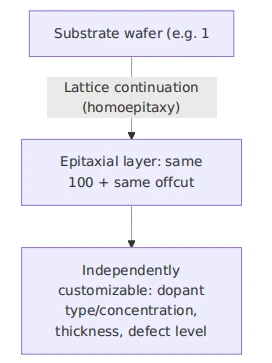
Silicon epitaxy is homoepitaxy (Si on Si): during growth, silicon atoms continue the substrate lattice atom by atom rather than
nucleating anew. The interface between the epitaxial layer and the substrate is therefore coherent and grain-boundary-free, and the
crystal orientation carries over naturally:
- 〈100〉 substrate → 〈100〉 epitaxial layer
- 〈111〉 substrate → 〈111〉 epitaxial layer
- The substrate offcut (miscut) is also inherited in full by the epitaxial layer
| Parameter | Inherited from substrate? | Explanation |
| Orientation/ offcut | Fully inherited | Coherent lattice, no grain boundary at the interface |
| Dopant type and concentration | Independently designed | Structures such asP/P+,N/N+,N/P; resistivity tailored to device requirements |
| Defect level | Independently controlled | Epitaxy may introduce stacking faults, sliplines, dislocations and haze; substrate defects can also propagate upward |
| Thickness and surface quality | Independently controlled | Thickness,uniformity and flatness are core epitaxial-layer metrics |
| Stress |
⚠Minor
|
Lattice-constant differences from heavily doped substrates introduce interface stress, but both sides remain the same silicon single-crystal system |
2. Is the 〈110〉 orientation inherited as well?
Yes. Orientation inheritance is a general rule of homoepitaxy, regardless of the specific orientation indices - if the substrate is〈110〉, the epitaxial layer is 〈110〉, and the offcut is inherited together with it.
Some practical points about 〈110〉 silicon wafers:
- A non-mainstream specification: The market mainstream is 〈100〉 (CMOS, power devices), while 〈111〉 is used for some bipolar devices and MEMS. 〈110〉 is mainly used for MEMS structural elements and high-frequency/specialty devices, valued for its distinctive anisotropic-etch behavior and carrier-transport properties.
- Harder epitaxy: The atomic arrangement of the 〈110〉 plane differs from 〈100〉; the process windows for growth rate, surface-morphology control and defect control are narrower, placing greater demands on the supplier's process capability.
- Scarce supply and long lead times: Few manufacturers mass-produce 〈110〉 substrates, and epitaxy capacity is likewise limited. Before purchasing, confirm substrate availability and the production scheduling cycle.
One sentence to remember: regardless of orientation, the epitaxial layer always "follows the substrate"; what can be customized is doping, thickness and defect level - never the orientation.
3. Is there any etching difference between a 〈110〉 epitaxial wafer and a 〈110〉 plain polished wafer?
Core conclusion: if what is being etched is the epitaxial layer, the orientation-related etching behavior is identical - anisotropic etching recognizes crystal planes, not whether the wafer was "grown" or "sliced". The real differences arise from doping levels and material quality.
1. The part determined by orientation: the same for both
In anisotropic wet etching with KOH, TMAH and similar chemistries, etch rates vary by crystal plane. On a 〈110〉 wafer, the {111} planes intersect the surface at approximately 90°, allowing near-vertical deep trenches and sidewalls to be etched - the main reason MEMS designers choose 〈110〉 material. The epitaxial layer inherits the 〈110〉 orientation and offcut, so etch angles, sidewall morphology and convex/concave-corner behavior match those of a 〈110〉 polished wafer.
2. Differences in actual etching results: rooted in the epitaxial layer itself
| Aspect | <110> epitaxial wafer | <110> plain polished wafer |
| Orientation-related etch behavior | Same(vertical sidewallcapability) | Same |
| Etch-stop structure | A heavily doped substrate plus lightly doped epitaxial layer enables P etch stopping for precise thickness control | Uniform doping throughout; no inter-layer etch stop possible |
| Etched surface quality | Cop-free, low oxygen, few bulk defects; cleaneretched surface with fewer pinholes/orange-peel effects | Oxygen precipitates and swirldefects may be present; defects tend to show up after etching |
| within-wafer uniformity | Excellent resistivity uniformity; consistent batch etch rates | Relatively weaker consistency |
| Structural-layer thickness | The epitaxial-layer thickness is the device structural-layer thickness, with high precision | Relies on thinning/mechanical control; precision one grade lower |
3. Dry etching (ICP/DRIE): essentially no difference
Plasma etching is a non-crystal-plane-selective process; 〈110〉 epitaxial and plain wafers behave almost identically, with differences limited to minor doping-related loading effects and surface defects.
Summary: In terms of "orientation etch characteristics", there is no difference; in terms of "etch precision, surface quality and etch-stop capability", the 〈110〉 epitaxial wafer is clearly superior - which is exactly why MEMS customers are willing to pay more for it.
4. Price ranges for 12-inch 〈110〉 epitaxial and polished wafers
Reference ranges (Prime grade, standard thickness, standard doping, volume orders)
| Product type | USD reference(per wafer) | RMB reference (per wafer,excl. VAT) |
| 12" <100> plain polished wafer (benchmark) | $200-500 | ¥1,500-3,500 |
| 12" <110> plain polished wafer | $400-900 | ¥3,000-6,500 |
| 12" <110> epitaxialwafer | $700-1,500 | ¥5,000-11,000 |
Pricing logic (more reliable than the specific numbers):
1. An epitaxial wafer ≈ substrate price + epitaxy processing fee. Standard 12-inch epitaxy processing typically costs $150‒400 per wafer; for 〈110〉, both substrate and processing carry premiums due to the narrow process window and lower yield.
2. The 〈110〉 premium is real: During 300mm 〈110〉 single-crystal growth, anisotropy easily leads to warpage, cracking and dislocations, with low slicing-and-polishing yields. Few manufacturers worldwide can mass-produce it; pricing is typically about 2× or more versus the equivalent 〈100〉 specification.
3. Small-batch / R&D wafer prices can double: Orders under 25 wafers require separate scheduling and process tuning; 〈110〉 epitaxial wafers above $2,000 per unit are not uncommon.
4. Main price variables: offcut precision (±0.5° vs ±0.1°), resistivity range, epitaxial-layer thickness and uniformity, particle/defect grade, and whether double-side polishing or special backside treatment is required.
Procurement advice: The real bottleneck for 12-inch 〈110〉 is often not price but availability and lead time - major international manufacturers mostly take orders on a project basis, with lead times of 4‒6 months or more. Meanwhile, a large share of 〈110〉 MEMS demand is actually concentrated at 6-inch/8-inch, where supply is mature and costs lower (6-inch 〈110〉 polished wafers run about $50‒150, epitaxial wafers about $150‒400). At the selection stage it is worth confirming first whether line width and capacity truly mandate 12-inch material.
Conclusion
- In homoepitaxy, the epitaxial layer inherits 100% of the substrate orientation and offcut, including for 〈110〉; doping, thickness and defect level are what can be customized.
- The core value of 〈110〉 material lies in its vertical-sidewall forming capability in anisotropic MEMS etching; the epitaxial wafer adds etch stopping, low defects and high uniformity on top.
- 12-inch 〈110〉 is a typical low-volume, project-based product - high-priced, long-lead-time and supply-constrained.
Evaluating 6/8-inch alternatives in parallel is recommended during device selection.
Ningbo Sibranch Microelectronics Technology Co., Ltd. focuses on semiconductor wafer supply, offering the full product range including polished wafers and epitaxial wafers together with selection and technical support. For special orientations such as 〈110〉 or small-volume R&D requirements, contact us for customized quotations and lead-time solutions.
- Websites: www.sibranch.com | www.sibranchwafer.com
- Keywords: silicon epitaxial wafer, substrate crystal orientation, 〈110〉 silicon wafer, MEMS wafer, anisotropic etching, 300mm epitaxial wafer, silicon wafer procurement


