


Product Description
One of the primary benefits of gallium arsenide substrate is its high electron mobility. It has a larger electron mobility compared to other semiconductor materials like silicon, which makes it ideal for high-speed, low-noise devices. Moreover, it has a direct bandgap that enables it to produce efficient light-emitting diodes that emit in the visible and infrared regions.
Another advantage of this substrate is its high thermal conductivity, which helps in dissipating heat quickly. This feature is especially useful in power electronics applications where heat dissipation is critical. Gallium arsenide substrate also has a high breakdown voltage, which ensures its reliability even under high voltage conditions.
|
Standard Dimensions and Tolerances for 150mm Diameter GaAs Wafer |
|||
|
Property |
Dimension |
Tolerance |
Units |
|
Diameter |
150 |
+/-0.5 |
mm |
|
Thickness, Center Point |
|||
|
Option A |
675 |
+/-25 |
μm |
|
Option B |
550 |
+/-25 |
μm |
|
Notch Orientation |
[010] |
+/-2 |
degrees |
|
Notch Depth |
1 |
+0.25/-0.0 |
mm |
|
Standard Dimensions and Tolerances for 100mm Diameter GaAs Wafer |
|||
|
Property |
Dimension |
Tolerance |
Units |
|
Diameter |
100 |
+/-0.5 |
mm |
|
Thickness, Center Point |
675 |
+/-25 |
μm |
|
Primary Flat Lenght |
18 |
+/-2 |
mm |
|
Secondary Flat Lenght |
18 |
+/-2 |
mm |
|
US/SEMI and E/J-Flat-Option available |
|||
|
Standard Dimensions and Tolerances for 200mm Diameter GaAs Wafer |
|||
|
Property |
Dimension |
Tolerance |
Units |
|
Diameter |
200 |
+/-0.5 |
mm |
|
Thickness, Center Point |
625 |
+/-25 |
μm |
|
Notch Orientation |
[010] |
+/-2 |
degrees |
|
Notch Depth |
1 |
+0.25/-0.0 |
mm |
|
Standard Dimensions and Tolerances for 3 inch Diameter GaAs Wafer |
|||
|
Property |
Dimension |
Tolerance |
Units |
|
Diameter |
76.2 |
+/-0.5 |
mm |
|
Thickness, Center Point |
625 |
+/-25 |
μm |
|
Primary Flat Lenght |
22 |
+/-2 |
mm |
|
Secondary Flat Lenght |
11 |
+/-2 |
mm |
|
US/SEMI and E/J-Flat-Option available |
|||
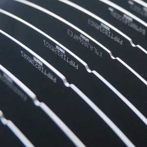
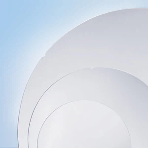
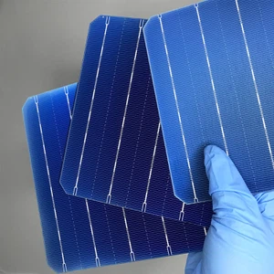
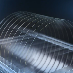
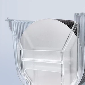
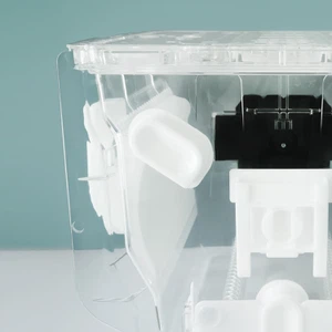
Product Picture


Why Choose Us
Our products are sourced exclusively from the world's top five manufacturers and leading domestic factories. Supported by highly skilled domestic and international technical teams and stringent quality control measures.
Our objective is to provide customers with comprehensive one-on-one support, ensuring smooth channels of communication that are professional, timely, and efficient. We offer a low minimum order quantity and guarantee swift delivery within 24 hours.
Factory Show
Our vast inventory consists of 1000+ products, ensuring that customers can place orders for as little as one piece. Our self-owned equipments for dicing & backgrinding, and full cooperation in the global industrial chain enable us prompt shipment to ensure customer one-stop satisfaction and convenience.


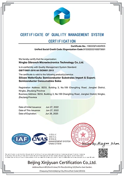
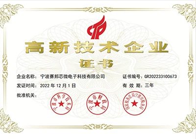
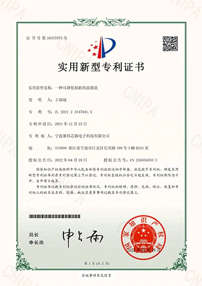
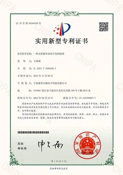
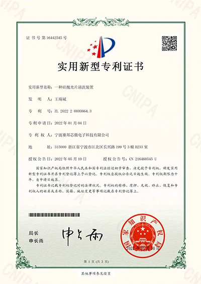
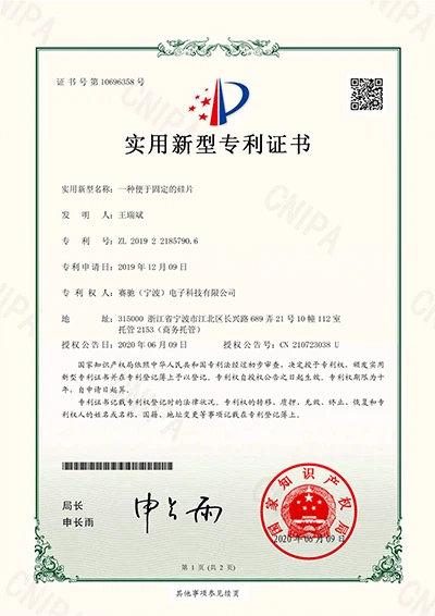
Our Certificate
Our company takes pride in the various certifications we have earned, including our patent certificate, ISO9001 certificate, and National High-Tech Enterprise certificate. These certifications represent our dedication to innovation, quality management, and commitment to excellence.


Hot Tags: gallium arsenide substrate, China gallium arsenide substrate manufacturers, suppliers, factory, Gallium Arsenide, Gallium Arsenide


