


Product Description
Gallium arsenide (GaAs) crystals have good chemical stability and hardness to withstand harsh environments. GaAs is available in ingots and polished wafers, conductive and semi-insulating GaAs wafers, mechanical grade and epitaxial grade.
Applications of Gallium Arsenide Wafer
- Light-emitting diodes
- Laser diodes
- Photovoltaic devices
- High Electron Mobility Transistor
- Heterojunction Bipolar Transistor

|
Standard Dimensions and Tolerances for 150mm Diameter GaAs Wafer |
|||
|
Property |
Dimension |
Tolerance |
Units |
|
Diameter |
150 |
+/-0.5 |
mm |
|
Thickness, Center Point |
|||
|
Option A |
675 |
+/-25 |
μm |
|
Option B |
550 |
+/-25 |
μm |
|
Notch Orientation |
[010] |
+/-2 |
degrees |
|
Notch Depth |
1 |
+0.25/-0.0 |
mm |
|
Standard Dimensions and Tolerances for 100mm Diameter GaAs Wafer |
|||
|
Property |
Dimension |
Tolerance |
Units |
|
Diameter |
100 |
+/-0.5 |
mm |
|
Thickness, Center Point |
675 |
+/-25 |
μm |
|
Primary Flat Lenght |
18 |
+/-2 |
mm |
|
Secondary Flat Lenght |
18 |
+/-2 |
mm |
|
US/SEMI and E/J-Flat-Option available |
|||
|
Standard Dimensions and Tolerances for 200mm Diameter GaAs Wafer |
|||
|
Property |
Dimension |
Tolerance |
Units |
|
Diameter |
200 |
+/-0.5 |
mm |
|
Thickness, Center Point |
625 |
+/-25 |
μm |
|
Notch Orientation |
[010] |
+/-2 |
degrees |
|
Notch Depth |
1 |
+0.25/-0.0 |
mm |
|
Standard Dimensions and Tolerances for 3 inch Diameter GaAs Wafer |
|||
|
Property |
Dimension |
Tolerance |
Units |
|
Diameter |
76.2 |
+/-0.5 |
mm |
|
Thickness, Center Point |
625 |
+/-25 |
μm |
|
Primary Flat Lenght |
22 |
+/-2 |
mm |
|
Secondary Flat Lenght |
11 |
+/-2 |
mm |
|
US/SEMI and E/J-Flat-Option available |
|||
Product Picture


Key Benefits of Gallium Arsenide Wafer:
High Electron Mobility: GaAs wafers have higher electron mobility than silicon, enabling faster device operation and higher frequency capabilities. This property is critical for applications that require high-speed signal processing, such as wireless communication systems and high-speed data transmission.
Low Resistivity: GaAs wafers have lower resistivity than silicon, which reduces the resistance encountered by charge carriers, which is critical for high-speed devices because it minimizes power loss and signal attenuation. Lower resistivity also enables efficient charge transport and enables devices to operate at higher speeds while improving power efficiency.
Wide Bandgap: Wider bandgap enables the production of high-performance optoelectronic devices. These devices include light-emitting diodes (LEDs), laser diodes, and photodetectors for applications such as optical communications, display technology, and solid-state lighting. In addition, wide bandgap can also emit and detect light over a wider range of wavelengths, thereby improving device performance and efficiency.
Low Noise Performance: Such wafers have inherently low noise characteristics, suitable for applications that require a high signal-to-noise ratio. This is important in areas such as telecommunications and radio frequency (RF) systems, where signal integrity and sensitivity are critical.
Thermal Stability: With excellent thermal stability, they can withstand high operating temperatures without significant performance degradation. These chips are therefore suitable for applications where high power dissipation and thermal management are critical.
GaAs Wafers' Utilization In Semiconductors & Computers
Gallium arsenide wafer, a parallel compound framed from the component gallium and arsenic, presents fabricating difficulties in the creation of semiconductors because of its lower warm conductivity and higher coefficient of warm extension (CTE) contrasted with rudimentary semiconductors like silicon and germanium. Also, understanding gadget disappointments in view of GaAs can be more perplexing and exorbitant than those in light of silicon because of its somewhat ongoing reception. In any case, while thinking about the equilibrium of value, cost, and the additional worth of GaAs, these confusions are offset. The developing business sectors, requesting innovation that empowers higher frequencies, add to the offset of these expenses.
GaAs Wafers' Utilization In Guard & Aerospace
Gallium arsenide has been integrated into business marketssince its utilization started for the military and aviation field. It has a place with the semiconductor materials bunch in the occasional table. The width of the band hole is more noteworthy than in silicon or germanium. The portability of the electrons is additionally more noteworthy than in silicon or germanium, and that of the openings like those of silicon.
To impurify the sort p, materials, for example, zinc, cadmium or copper are utilized since they present allowed levels in the scope of 0.08 to 0.37 eV over the valence band of GaAs. The giver materials are sulfur, selenium and the components of gathering IV of the occasional table, in little fixation, assuming they supplant gallium particles.
The GaAs is utilized for photoelectric cells, burrowing diodes, lasers, semiconductors and MESFET semiconductors.
The GaAs has a few circuit geographies and gadget types. The most predominant and industrially accessible is the FET rationale straightforwardly combined with DCFL (Direct Coupled FET Rationale), in spite of the fact that BFL rationale (Cradled FET Rationale) and SDFL rationale (Schottky Diode FET Rationale) are likewise accessible
GaAs Wafers Use In High Recurrence Technologies
The powerful mass of the electric charge of the doped N-type GaAs is lower than in the silicon of a similar kind, so the electrons in GaAs Wafers are advanced at higher velocities, getting some margin to cross the semiconductor channel. This is extremely helpful at high frequencies, since a higher greatest working recurrence will be reached.
This chance and need to work with circuits that permit to act at higher frequencies has its starting point in the guard and space enterprises, in the utilization of radars, secure correspondences and sensors. After advancement by government programs, GaAs before long extended to new ad showcases, for example, remote neighborhood (WLAN), individual correspondence frameworks (laptops), live satellite transmission (DBS), transmission and gathering by the shopper, worldwide situating frameworks (GPS) and versatile interchanges. This multitude of business sectors required working at high and low frequencies that couldn't be accomplished with silicon or germanium.
Why Choose Us
Our products are sourced exclusively from the world's top five manufacturers and leading domestic factories. Supported by highly skilled domestic and international technical teams and stringent quality control measures.
Our objective is to provide customers with comprehensive one-on-one support, ensuring smooth channels of communication that are professional, timely, and efficient. We offer a low minimum order quantity and guarantee swift delivery within 24 hours.
Factory Show
Our vast inventory consists of 1000+ products, ensuring that customers can place orders for as little as one piece. Our self-owned equipments for dicing & backgrinding, and full cooperation in the global industrial chain enable us prompt shipment to ensure customer one-stop satisfaction and convenience.


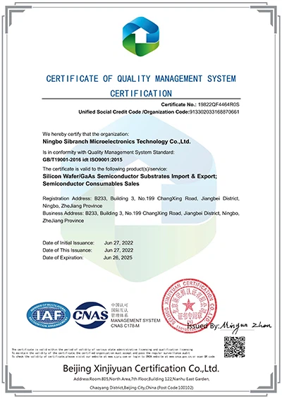
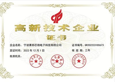
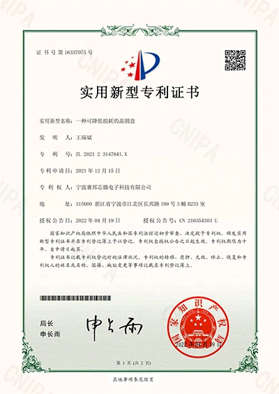
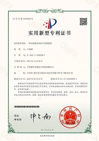
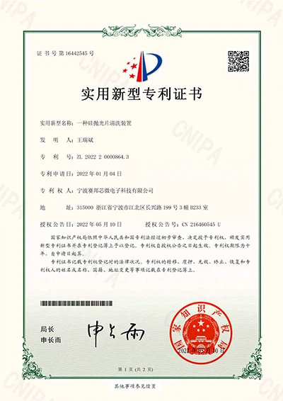
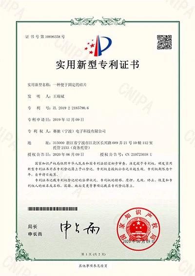
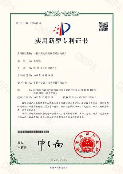
Our Certificate
Our company takes pride in the various certifications we have earned, including our patent certificate, ISO9001 certificate, and National High-Tech Enterprise certificate. These certifications represent our dedication to innovation, quality management, and commitment to excellence.


Hot Tags: gallium arsenide wafer, China gallium arsenide wafer manufacturers, suppliers, factory


