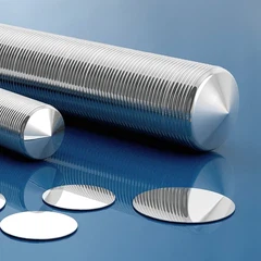
Ultra-high resistance zone fused silicon single crystal (FZ-Silicon)
Silicon single crystal with low impurity content, low defect density and perfect lattice structure drawn by zone melting process, no impurities are introduced during the crystal growth process, and its resistivity is usually above 1000Ω?cm, mainly used to produce high back pressure devices and optoelectronic devices.
Fused silicon single crystal in neutron irradiation zone (NTDFZ-Silicon)
Zone-melted silicon single crystals can obtain silicon single crystals with high resistivity uniformity through neutron irradiation, which ensures the yield and consistency of device manufacturing. Mainly used in the production of silicon rectifiers (SR), thyristors (SCR), giant transistors (GTR), thyristors (GRO), static induction thyristors (SITH), insulated gate bipolar transistors (IGBT), ultra-high voltage diodes (PIN), Smart power devices (SMART POWER), power integrated devices (POWER IC), etc., are the main functional materials of various frequency converters, rectifiers, high-power control devices, and new power electronic devices, as well as a variety of detectors, sensors, optoelectronic devices and Main functional materials for special power devices, etc.
Gas phase doped zone fused silicon single crystal (GDFZ-Silicon)
Utilizing the diffusion mechanism of impurities, gaseous impurities are added in the process of drawing silicon single crystal by zone melting process, which fundamentally solves the problem of difficult doping in zone melting process, and can obtain N-type or P-type, resistivity range 0.001- 300Ω.cm, gas-doped silicon single crystal with resistivity uniformity equivalent to that of neutron irradiation, its resistivity is suitable for making various semiconductor power devices, insulated gate bipolar transistors (IGBT), high-efficiency solar cells, etc.
Czochralski zone fused silicon single crystal (CFZ-Silicon)
The silicon single crystal is drawn by the combination of two processes of Czochralski and zone melting, and the product quality is between the Czochralski and zone melting single crystal. Special elements such as gallium (Ga), germanium (Ge), etc. can be doped. The new generation of CFZ solar silicon wafers prepared by the Czochralski zone melting method are far superior to all kinds of silicon wafers currently used in the global photovoltaic industry, and the conversion efficiency of solar cells is as high as 24-26%. The products are mainly used in high-efficiency solar cells made of special structures, back contacts, HIT and other special processes, and are more widely used in many products and fields such as LEDs, power devices, automobiles, and satellites.
What Is Zone Fused Silicon Single Crystal Wafer?
Jul 02, 2023Leave a message


