


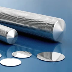




Polished wafers are the most used product, and other silicon wafer products are produced by secondary processing on the basis of polished wafers.
Polished wafers are the most basic and widely used silicon wafers. Polished wafers can be directly used to make semiconductor devices, widely used in memory chips and power devices, and can also be used as substrate materials for epitaxial wafers, SOI silicon wafers and other types of silicon wafers.
With the continuous shrinking of the characteristic line width of integrated circuits and the increasingly finer precision of lithography, the extremely small unevenness on the silicon wafer will cause the deformation and dislocation of the integrated circuit graphics. The silicon wafer manufacturing technology is facing higher and higher requirements and challenges. Chip surface particle size and cleanliness also have a direct impact on the yield of semiconductor products.
Therefore, the polishing process is very important to improve the flatness and cleanliness of the silicon wafer surface. The main principle is to achieve the planarization of the semiconductor silicon wafer surface and reduce the roughness by removing the residual damage layer on the processed surface.
Where are silicon wafer polishing pads used?
Jul 16, 2023
Leave a message
You Might Also Like


