






In the chip manufacturing process, the term "SOI" is often heard. And chip manufacturing also usually uses SOI substrates to manufacture integrated circuits. The unique structure of SOI substrates can greatly improve the performance of chips, so what exactly is SOI? What are its advantages? In what fields is it used? How is it manufactured?

What is an SOI substrate?
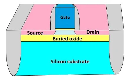
SOI is the abbreviation of Silicon-On-Insulator. It literally means silicon on an insulating layer. The actual structure is that there is an ultra-thin insulating layer, such as SiO2, on the silicon wafer. There is another thin silicon layer on the insulating layer. This structure separates the active silicon layer from the silicon layer of the substrate. In the traditional silicon process, the chip is formed directly on the silicon substrate without using an insulator layer.

What are the advantages of SOI substrate?
Low substrate leakage current
Due to the presence of an insulating layer of silicon oxide (SiO2), it effectively isolates the transistor from the underlying silicon substrate. This isolation reduces undesired current flow from the active layer to the substrate. Leakage current increases with temperature, so the reliability of the chip can be significantly improved in high-temperature environments.
Reduce parasitic capacitance
In the SOI structure, the parasitic capacitance is significantly reduced. Parasitic capacitances often limit speed and increase power consumption, so they add extra delay during signal transmission and consume extra energy. By reducing these parasitic capacitances, applications are common in high-speed or low-power chips. Compared with ordinary chips made in the CMOS process, the speed of SOI chips can be increased by 15% and the power consumption can be reduced by 20%.
Noise Isolation
In mixed-signal applications, noise generated by digital circuits may interfere with analog or RF circuits, thereby degrading system performance. Since the SOI structure separates the active silicon layer from the substrate, it actually achieves a kind of inherent noise isolation. This means that it is more difficult for noise generated by digital circuits to propagate through the substrate to sensitive analog circuits.
How to manufacture SOI substrate?
There are generally three methods: SIMOX, BESOI, crystal growth method, etc. Due to limited space, here we introduce the more common SIMOX technology.
SIMOX, the full name of Separation by IMplantation of OXygen, is to use oxygen ion implantation and subsequent high-temperature annealing to form a thick silicon dioxide (SiO2) layer in the silicon crystal, which serves as the insulator layer of the SOI structure.

High-energy oxygen ions are implanted into a specific depth in the silicon substrate. By controlling the energy and dosage of the oxygen ions, the depth and thickness of the future silicon dioxide layer can be determined. The silicon wafer implanted with oxygen ions undergoes a high-temperature annealing process, usually between 1100°C and 1300°C. At this high temperature, the implanted oxygen ions react with the silicon to form a continuous silicon dioxide layer. This insulating layer is buried under the silicon substrate, forming an SOI structure. The surface silicon layer becomes the functional layer for manufacturing the chip, while the silicon dioxide layer below acts as an insulator layer, isolating the functional layer from the silicon substrate.
In which chips are SOI substrates used?
They can be used in CMOS devices, RF devices, and silicon photonic devices.
What are the common thicknesses of each layer of SOI substrates?

Silicon substrate layer thickness: 100μm / 300μm / 400μm / 500μm / 625μm ~ and above
SiO2 thickness: 100 nm to 10μm
Active silicon layer: ≥20nm


